
Sintered silver microparticle compact

一种银微粒、烧结体的技术,应用在导体、非绝缘导体、电固体器件等方向,能够解决层间绝缘膜应力破损等问题,达到抑制裂纹、高导热率、高生产率和经济性的效果

Active Publication Date: 2014-11-19
NAMICS CORPORATION
View PDF9 Cites 4 Cited by
  • Summary
  • Abstract
  • Description
  • Claims
  • Application Information

AI Technical Summary

Problems solved by technology

In addition, in flip-chip semiconductors, there is a problem of damage caused by stress due to the lowering of the dielectric constant of the interlayer insulating film.

Method used


Image

  • Sintered silver microparticle compact
  • Sintered silver microparticle compact
  • Sintered silver microparticle compact

Examples


Embodiment

[0096] The silver fine particle sintered body of the present invention was trial-produced in the following procedure. That is, first, a conductive paste containing silver fine particles is prepared, and then the conductive paste is printed on a slide glass and fired.

[0097] The manufacturing method of the silver fine particle containing conductive paste of Examples 1-3 and Comparative Examples 1 and 2 is as follows. 3.0 kg (30.9 mol) of 3-methoxypropylamine was added to a 10 L glass reaction vessel. While stirring, the reaction temperature was kept below 45° C., and 5.0 kg (30.0 mol) of silver acetate was added. Immediately after the addition, it was dissolved as a transparent solution, but as the addition progressed, the solution gradually became cloudy, and when the entire amount was added, it became a viscous solution of a gray-tea turbid color. 1.0 kg (21.0 mol) of 95% by weight formic acid was slowly added dropwise thereto. Immediately after the dropwise addition, in...

Embodiment 4

[0124] Next, the silver fine particle sintered body of Example 4 was produced in the same manner as in Example 1 except that an epoxy resin as a curable resin was further mixed with the conductive paste of Example 1 and fired. The silver fine particle sintered body of Example 4 contained curable resin. Diglycidyl hexahydrophthalate was used for the epoxy resin. Moreover, the addition amount of an epoxy resin was 3.5 weight part with respect to 100 weight part of silver fine particles.

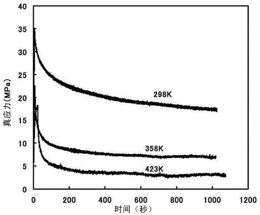
[0125] exist Figure 11 The results of the stress relaxation test of the curable resin-containing silver particle sintered body of Example 4 are shown in . It should be noted that, for comparison, in Figure 11 The stress relaxation test results of the silver particle sintered body of Example 1 are also shown in . Depend on Figure 11 It is clear that the same stress relaxation behavior as that of the silver fine particle sintered body of Example 1 was observed in the curable resin-contain...


PUM

PropertyMeasurementUnit
particle diameteraaaaaaaaaa
melting pointaaaaaaaaaa

Abstract

A sintered silver microparticle compact for a joint material that is used for the joining of a part of a semiconductor device, said sintered silver microparticle compact having such properties that the activation energy for the creeping of the sintered silver microparticle compact is 0.4- to 0.75-fold of the activation energy for the lattice diffusion of bulk silver.

Description

technical field [0001] The present invention relates to a silver fine particle sintered body that can be used as a bonding member for bonding components of a semiconductor device when manufacturing a semiconductor device, and a method for manufacturing the same. In particular, the present invention relates to a silver fine particle sintered body that can be used as a bonding member such as a bump and a die attach, and a method for producing the same. Background technique [0002] Along with miniaturization, weight reduction, and higher performance of electronic equipment, the amount of heat generated by semiconductor devices increases and the heat density increases. In addition, in flip-chip semiconductors, there is a problem of damage due to stress due to lowering of the dielectric constant of the interlayer insulating film. In addition, semiconductors with large band gaps such as silicon carbide and gallium nitride are being studied as power semiconductors. Power semicon...

Claims


Application Information

Patent Timeline
Patent Type & Authority Applications(China)
IPC IPC(8): H01L21/52B22F1/00B22F7/08B22F9/24H01B5/00H01L21/60B22F1/054
CPCB82Y30/00H01L2224/29339H01L24/83H01L2224/8184B22F1/00H01L24/29H01L24/13B22F9/24H01L2224/13499B22F3/10H01L2924/13091B22F1/0018H01L2224/13339C22C5/06H01L24/32H01L2224/8384H01L24/16H01L2224/29499H01L24/81B22F1/054B22F1/056H01L2924/00H01L2924/207H01L2924/12042B23K35/3006B23K35/365H01L2224/11505H01L24/11B22F1/07B23K1/0016H01L2224/165H01L2924/01047
Inventor 小林诚佐佐木幸司
Owner NAMICS CORPORATION
Learn More