GaN-based enhancement/depletion mode heterojunction field effect transistor with buried gate structure

A heterojunction field effect, gallium nitride-based technology, applied in semiconductor devices, electrical components, circuits, etc., can solve the problems of material reliability, difficulty in realizing P-type GaN materials, and high activation energy, so as to avoid disadvantages effect, high maximum saturation leakage current, simple manufacturing process

Active Publication Date: 2014-11-26
UNIV OF ELECTRONICS SCI & TECH OF CHINA
View PDF4 Cites 11 Cited by
  • Summary
  • Abstract
  • Description
  • Claims
  • Application Information

AI Technical Summary

Problems solved by technology

However, the P-type acceptor Mg activation energy of GaN materials is very high, and it is difficult to realize high-quality P-type GaN materials. At the same time, P-type doping will also affect the reliability of the material.

Method used


Image

  • GaN-based enhancement/depletion mode heterojunction field effect transistor with buried gate structure
  • GaN-based enhancement/depletion mode heterojunction field effect transistor with buried gate structure
  • GaN-based enhancement/depletion mode heterojunction field effect transistor with buried gate structure

Examples


Embodiment

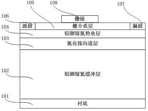
[0037] figure 1 It is a prior art GaNHFET structure, mainly including substrate 101, aluminum indium gallium nitride (Al x In y Ga z N) buffer layer 102, gallium nitride (GaN) channel layer 103, aluminum indium gallium nitride (Al x In y Ga z N) Barrier layer 104, gate dielectric layer 105, aluminum gallium nitride (Al x In y Ga z N) The source electrode 106 and the drain electrode 107 formed on the barrier layer 104, and the gate electrode 108 formed on the barrier dielectric layer 105, wherein the source electrode 106 and the drain electrode 107 are combined with aluminum indium gallium nitride (Al x In y Ga z N) The barrier layer 104 forms an ohmic contact, and the gate 108 forms a Schottky contact with the gate dielectric layer 105 .

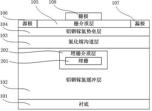
[0038] figure 2 The structure schematic diagram of GaN-based enhanced depletion heterojunction field effect transistor with buried gate structure provided by the present invention mainly consists of substrate 101, AlInGaN buffer ...


PUM


Abstract

The invention discloses a GaN-based enhancement/depletion mode heterojunction field effect transistor with a buried gate structure. The GaN-based enhancement/depletion mode heterojunction field effect transistor is mainly composed of a substrate, an AlInGaN buffer layer, a buried gate, a buried gate dielectric layer, a GaN channel layer, an AlInGaN barrier layer, a gate dielectric layer, a source electrode, a drain electrode and a gate electrode from bottom to top, wherein the source electrode and the drain electrode are arranged on the AlInGaN barrier layer, and the gate electrode is arranged on the gate dielectric layer. The source electrode and the drain electrode are in ohmic contact with the AlInGaN barrier layer, and the source electrode and the gate dielectric layer are in Schottky contact. The buried gate dielectric layer and the buried gate are both placed in the AlInGaN buffer layer, and the buried gate is placed in the buried dielectric layer. Through independent bias arrangement of the buried gate, according to the different bias arrangement of the buried gate, the threshold voltage of devices is adjusted; when the buried gate is in a negative bias state, two-dimensional electron gas in the AlInGaN barrier layer is exhausted by the buried gate, and the devices are made to achieve enhancement mode work; when the buried gate is in a zero bias state or a positive bias state, the two-dimensional electron gas exists in the AlInGaN barrier layer, and the devices are made to achieve depletion mode work.

Description

technical field [0001] The invention relates to the field of semiconductor devices, in particular to a gallium nitride-based enhanced depletion heterojunction field effect transistor with a buried gate structure. Background technique [0002] Gallium nitride (GaN)-based heterojunction field effect transistor has excellent characteristics such as large band gap, high critical breakdown electric field, high electron saturation velocity, good thermal conductivity, radiation resistance and good chemical stability. At the same time, GaN ( GaN) materials can form a two-dimensional electron gas heterojunction channel with high concentration and high mobility with materials such as aluminum gallium nitride (ALGaN), so it is especially suitable for high-voltage, high-power and high-temperature applications, and is the most potential for electronic applications one of the transistors. [0003] figure 1 It is a schematic diagram of the structure of a common GaN-based heterojunction f...

Claims


Application Information

Patent Timeline
Patent Type & Authority Applications(China)
IPC IPC(8): H01L29/78H01L29/10H01L29/423
CPCH01L29/42356H01L29/778
Inventor 杜江锋潘沛霖陈南庭于奇
Owner UNIV OF ELECTRONICS SCI & TECH OF CHINA
Why Eureka
Try Eureka