Conductive paste for die bonding, and die bonding method using conductive paste for die bonding

A chip bonding and conductivity technology, applied in the field of conductive paste, can solve problems such as increased thermal stress, changes in the electrical characteristics of semiconductor chips, and the influence of semiconductor chip characteristics, and achieve the effect of improving durability

Inactive Publication Date: 2014-12-10
TANAKA PRECIOUS METAL IND
View PDF8 Cites 2 Cited by
  • Summary
  • Abstract
  • Description
  • Claims
  • Application Information

AI Technical Summary

Problems solved by technology

This is because if the bonding temperature is set at a high temperature, the thermal stress generated during cooling after bonding increases, and the electrical characteristics of the semiconductor chip may vary.
In addition, the heating itself at the time of bonding may also affect the characteristics of the semiconductor chip

Method used


Image

  • Conductive paste for die bonding, and die bonding method using conductive paste for die bonding
  • Conductive paste for die bonding, and die bonding method using conductive paste for die bonding
  • Conductive paste for die bonding, and die bonding method using conductive paste for die bonding

Examples


no. 1 approach

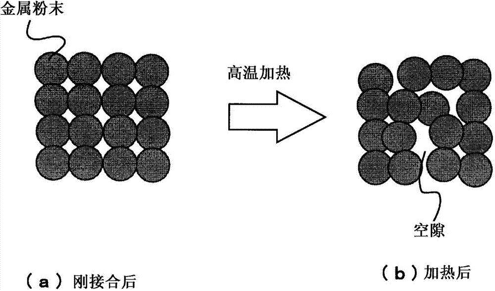
[0037] Here, a conductive paste obtained by dispersing a metal powder in which a coating layer made of gold is formed on a metal particle is produced, and the Si chip is die-bonded on a semiconductor substrate using the conductive paste. completeness research.

[0038] Manufacture of conductive paste :

[0039] Silver powder with a purity of 99.9% by mass (average particle diameter: 0.3 μm) produced by a wet reduction method was coated with gold as a coating layer. The formation of the coating layer is performed by an electroless plating method. Specifically, a non-cyanide displacement type electroless gold plating solution was used as the plating solution. As the gold source, a plating solution containing 5 g / L of gold sulfite was used as the gold concentration. As a pretreatment, use dilute sulfuric acid to remove oxides and sulfides on the surface of the silver powder. As the plating conditions, set the plating temperature to 70°C, put the silver powder into the platin...

no. 2 approach

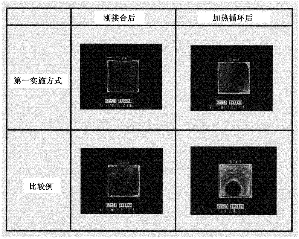
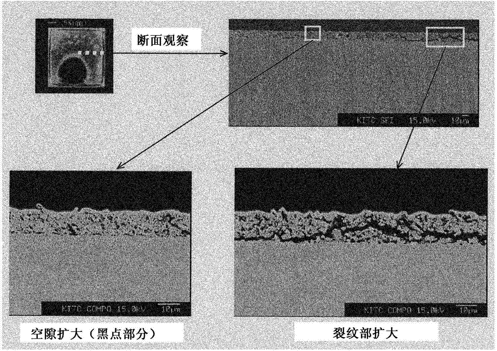
[0055] Here, two kinds of metal powders (silver powder and copper powder) with the thicknesses of the clad layers adjusted were prepared, a conductive paste was produced, and the soundness of the junction depending on the ratio of the clad layers was studied. The metal powder was produced in the same manner as in the first embodiment, changing the gold plating conditions as the cladding layer to achieve thicknesses of 0.001 μm, 0.002 μm, 0.005 μm, 0.05 μm, 0.1 μm, and 0.3 μm. Regarding the thickness of the coating layer, the plating conditions were changed so that the gold concentration of the plating solution was 2 to 10 g / L, the plating temperature was set at 60 to 90° C., and the plating time was 1 to 2 hours. In addition, the manufacture of the conductive paste is also the same as that of the first embodiment. In addition, Si chips were similarly bonded on the DBC substrate. In soundness evaluation of the joint between the Si chip and the DBC substrate, the shear strength...


PUM

PropertyMeasurementUnit
particle sizeaaaaaaaaaa
thicknessaaaaaaaaaa
particle sizeaaaaaaaaaa

Abstract

The present invention is a conductive paste for die bonding, which is composed of a metal powder and an organic solvent. The metal powder is composed of one or more kinds of metal particles having a purity of 99.9% by mass and an average particle diameter of 0.01-1.0 mum and selected from among a silver powder, a palladium powder and a copper powder, and coating layers that cover at least parts of the metal particles and are formed of gold. The conductive paste of the present invention is capable of suppressing the occurrence of defects such as voids at a bonded portion when a semiconductor element or the like is die-bonded to a substrate.

Description

technical field [0001] The present invention relates to a conductive paste suitable for chip bonding and flip chip bonding of a semiconductor chip onto a substrate, and a bonding method using the conductive paste. In particular, it relates to a highly durable conductive paste that does not generate voids in joints even after a long period of time at high temperatures. Background technique [0002] As a method of die-bonding various semiconductor chips onto a substrate, a method using solder has been known conventionally. In this die bonding method, after solder is fused to either a semiconductor chip or a substrate, the semiconductor chip is placed on the substrate, heated to a temperature equal to or higher than the melting point of the solder, and the solder is melted and solidified. The heating temperature (joining temperature) at this time is set in consideration of the melting point of the solder used. For example, AuSn-based solder is known as a solder commonly used ...

Claims


Application Information

Patent Timeline
Patent Type & Authority Applications(China)
IPC IPC(8): H01L21/52H01B1/00H01B1/22B22F1/107B22F1/17
CPCH01L2224/29339H01L2224/29444H01B1/22H01L2224/29294H01L2224/83203H01L24/32H01L24/83H01L2224/29347H01L2224/29364H01L24/29H01L2224/83192H01L2924/10253H01L2224/32225B22F1/17B22F1/107H01L2924/00H01L2924/01203H01L2924/351H01L2924/15747H01L2224/11416H01L2224/13444B23K35/3006B23K35/302B23K35/322B23K35/226H01L24/11H01L24/13H01L24/16H01L24/27H01L2224/0401H01L2224/04026H01L2224/05082H01L2224/05166H01L2224/05169H01L2224/05644H01L2224/11312H01L2224/11318H01L2224/1132H01L2224/13294H01L2224/13339H01L2224/13347H01L2224/13364H01L2224/16227H01L2224/27312H01L2224/2732H01L2224/27416H01L2224/81192H01L2224/81203H01L2224/81444H01L2224/8184H01L2224/83444H01L2224/8384H01L2224/27318B23K35/3013B23K35/0222B23K35/0244H01L24/81B23K2101/40B23K35/025H01L2924/01029H01L2924/01046H01L2924/01047H01L2924/01079H01L2924/00014H01L2924/00012B23K1/203H01L2924/014
Inventor 小柏俊典盐屋晶和宫入正幸
Owner TANAKA PRECIOUS METAL IND
Why Eureka
Try Eureka