Organic light emission diode device and fabrication method thereof

An electroluminescence device and electroluminescence technology, which are applied in the directions of organic semiconductor devices, materials of organic semiconductor devices, and electric solid devices, etc., and can solve the problems of poor light transmittance, poor light transmittance, and inability to emit light.

Inactive Publication Date: 2014-12-17
OCEANS KING LIGHTING SCI&TECH CO LTD +2
View PDF3 Cites 5 Cited by
  • Summary
  • Abstract
  • Description
  • Claims
  • Application Information

AI Technical Summary

Problems solved by technology

[0003] In traditional top-emitting OLED light-emitting devices, a semi-transparent metal film is usually used as a light-transmitting electrode. Due to the poor light transmission of the metal electrode itself, the light transmittance is poor, and there is a considerable part of the opti

Method used


Image

  • Organic light emission diode device and fabrication method thereof
  • Organic light emission diode device and fabrication method thereof
  • Organic light emission diode device and fabrication method thereof

Examples


Embodiment 1

[0052] A method for preparing an organic electroluminescent device, comprising the following steps:

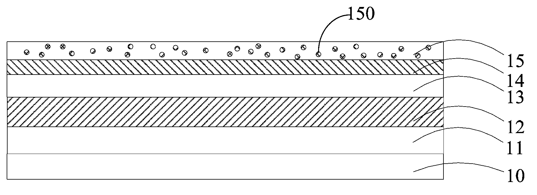
[0053] (1) Place a transparent glass substrate on a 1×10 -4 In the vacuum coating chamber of Pa, a metal Ag film with a thickness of 100nm is prepared on the surface of the substrate by vacuum evaporation as the anode;

[0054] (2) Prepare a light-emitting functional layer on the surface of the anode by vacuum evaporation, including a hole injection layer, a hole transport layer, a light-emitting layer, an electron transport layer, and an electron injection layer in sequence;

[0055] Among them, the hole injection layer is made of CuPc with a thickness of 20nm; the hole transport layer is made of NPB with a thickness of 30nm; the light emitting layer is made of Ir(ppy) 3 Doping mixed materials formed in CBP, where Ir(ppy) 3 The mass ratio to CBP is 10:100, and the thickness is 15nm; the electron transport layer uses TPBi, and the thickness is 30nm; the electron injection la...

Embodiment 2

[0061] The difference between this embodiment and Embodiment 1 is that the material of the light extraction layer includes titanium dioxide nano-microspheres and photocurable acrylic resin with a mass ratio of 20:100, the particle size of the titanium dioxide nano-microspheres is 100nm, and the screen printing process adopts mesh size A film was formed for 1000-mesh screen printing, and the thickness of the light extraction layer was 80 μm.

Embodiment 3

[0063] The difference between this embodiment and Example 1 is that the material of the light extraction layer includes titanium dioxide nano-microspheres and photocurable acrylic resin with a mass ratio of 20:100, the particle size of the titanium dioxide nano-microspheres is 250nm, and the screen printing process adopts mesh size The film was formed by 800-mesh screen printing, and the thickness of the light extraction layer was 20 μm.


PUM

PropertyMeasurementUnit
Particle sizeaaaaaaaaaa
Thicknessaaaaaaaaaa
Thicknessaaaaaaaaaa

Abstract

The invention provides an organic light emission diode device. The organic light emission diode device comprises a substrate and an anode, a light emission functional layer and a cathode which are sequentially laminated on the substrate, a light matching layer and a light extraction layer are sequentially arranged on the surface of the cathode, the material of the light extraction layer comprises nanoparticles and a polymer material, the nanoparticles are ceramic or high-polymer material particles with the grain size of 50 to 1,500 nanometers, the polymer material is a heat cured polymer or photo cured polymer material, the thickness of the light extraction layer is 10 to 100 micrometers, the material of the light matching layer is a mixed material formed by metal and an organic material, the metal is silver, aluminum or magnesium, and the organic material is N,N'-diphenyl-N,N'-bis(1-naphthyl)-1,1'-biphenyl-4,4'-diamine, copper phthalocyanine or 8- hydroxyquinoline aluminum. The luminous efficiency of the cathode of the organic light emission diode device is high, so that the luminous efficiency of the device is improved. The invention also provides a fabrication method of the organic light emission diode device.

Description

technical field [0001] The invention relates to an organic electroluminescent device, in particular to an organic electroluminescent device and a preparation method thereof. Background technique [0002] Organic Light Emission Diode, hereinafter referred to as OLED, has the characteristics of high brightness, wide range of material selection, low driving voltage, fully cured active light emission, etc., and has the advantages of high definition, wide viewing angle, and fast response speed. It is a display technology and light source with great potential, which conforms to the development trend of mobile communication and information display in the information age, as well as the requirements of green lighting technology, and is the focus of many researchers at home and abroad. [0003] In traditional top-emitting OLED light-emitting devices, a semi-transparent metal film is usually used as a light-transmitting electrode. Due to the poor light transmission of the metal electr...

Claims


Application Information

Patent Timeline
IPC IPC(8): H01L51/52H01L51/54H01L51/56
CPCH10K50/85H10K50/854H10K2102/00H10K71/00
Inventor 周明杰冯小明黄辉王平
Owner OCEANS KING LIGHTING SCI&TECH CO LTD
Why Eureka
Try Eureka