SOI horizontal power MOSFET device

A power and device technology, applied in the field of SOI lateral power MOSFET devices, can solve the problems of increased difficulty in extending the trench gate 8 process, little improvement in device on-resistance, and increased process complexity, so as to increase the auxiliary depletion effect, The effect of reducing the drift region and device length and reducing the cost of the chip

Inactive Publication Date: 2014-12-24
UNIV OF ELECTRONICS SCI & TECH OF CHINA
View PDF4 Cites 13 Cited by
  • Summary
  • Abstract
  • Description
  • Claims
  • Application Information

AI Technical Summary

Problems solved by technology

When the withstand voltage of the device is higher than 300V, on the one hand, this type of device requires a thicker active layer, which will inevitably lead to increased difficulty in the process of extending the trench gate 8, resulting in an increase in cost; on the other hand, a thicker dielectric buried layer 2, which will lead to serious self-heating effects; in addition, in high-voltage applications, the channel resistance accounts for a small proportion of the total device resistance, and the use of dual channels increases the process complexity, but does not improve the on-resistance of the device. Big
It can be seen that this type of device is not suitable for manufacturing power devices with a withstand voltage >300V

Method used


Image

  • SOI horizontal power MOSFET device
  • SOI horizontal power MOSFET device
  • SOI horizontal power MOSFET device

Examples


Embodiment 1

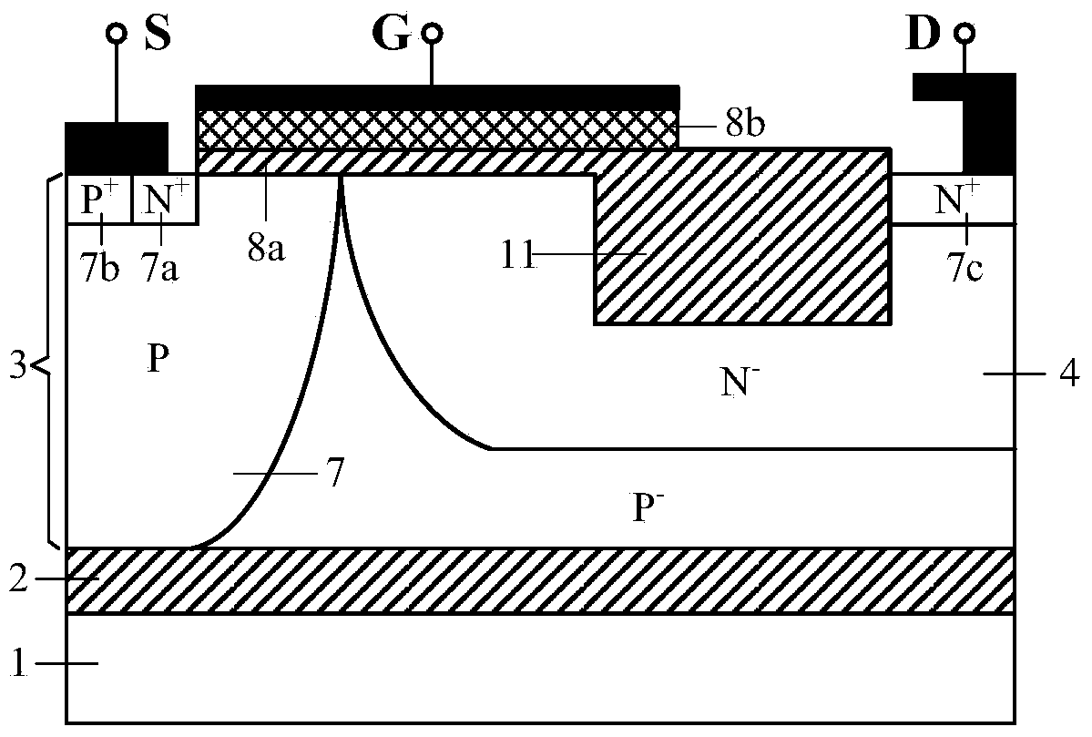
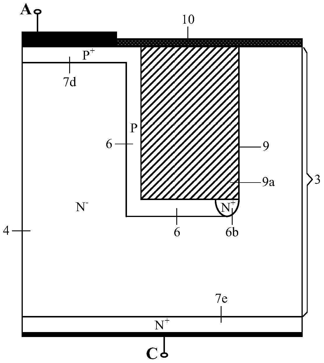
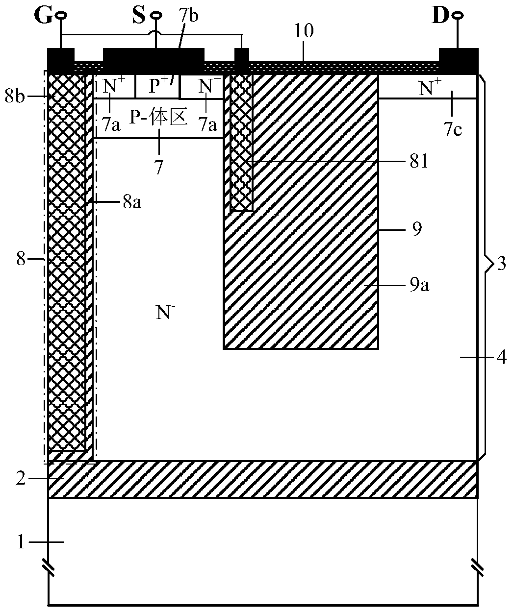
[0031] A SOI lateral power MOSFET device, such as Figure 4 , including a substrate layer 1 , a dielectric buried layer 2 and an active layer 3 from bottom to top. The active layer 3 is a semiconductor of the first doping type; one side of the active layer 3 has a semiconductor body region 7 of the second doping type, and the other side has a semiconductor drain region 7c of the first heavily doping type. The semiconductor body region 7 of the second doping type has a first heavily doped type semiconductor source region 7a and a second heavily doped type semiconductor body contact region 7b which are independent of each other, and the first heavily doped type semiconductor source region 7a and the second heavily doped semiconductor body region 7b are independent of each other. The leading end of the doubly doped type semiconductor body contact region 7b is connected to the metal source electrode S. As shown in FIG. The leading end of the drain region 7c of the first heavily d...

Embodiment 2

[0035] With the trench gate structure device in embodiment 1 (such as Figure 4 As shown in (a), compared with the device in this example, the groove gate 8 is extended to the dielectric buried layer 2, as shown in Figure 5 (a) shown. When the device proposed by the present invention is used in a high-voltage integrated circuit, the trench gate can realize full dielectric isolation between it and a low-voltage control circuit, which simplifies the manufacturing process of the integrated circuit. During forward conduction, the extended trench gate 8 can form an accumulation layer in the active layer 3, thereby greatly reducing the specific on-resistance. In the reverse blocking state, the extended trench gate 8, the dielectric buried layer 2 and the dielectric trench 9 can form a multi-dimensional depletion of the drift region 4, which can increase the concentration of the drift region and reduce the on-resistance on the other hand. It can also improve the withstand voltage ...

Embodiment 3

[0037] Compared with Example 2, the device of this example is implanted between the active layer 3 and the dielectric buried layer 4 to form a thinner N-type buffer layer 4a, such as Figure 5 (b) shown. The buffer layer 4 a and the extended groove gate 8 can form an L-shaped low-resistance current path, which can greatly reduce the specific on-resistance of the device.


PUM


Abstract

The invention provides an SOI horizontal power MOSFET device and belongs to the technical field of power semiconductor devices. A dielectric groove is introduced in a drift region and filled with two or more dielectric materials, and the dielectric coefficients of the dielectric materials are lower than the dielectric coefficient of an active layer and are gradually decreased from bottom to top; the side, close to a body region, of the dielectric groove is of a body region longitudinal extension structure; a semiconductor buried layer opposite to the drift region in doping type is arranged between the dielectric groove and a dielectric buried layer. Because the dielectric groove filled with the variable k dielectric materials has an modulating action on an internal electric field of the active layer and plays a role in longitudinally folding the drift region, the voltage resistance of the device is greatly improved, and the horizontal size of the device is reduced; because of introduction of the body region longitudinal extension structure and the semiconductor buried layer, the voltage resistance of the device is further improved, the exhausting action on the drift region is enhanced, the doping concentration of the drift region can be improved, and therefore the on resistance of the device is reduced; the grid and drain capacitance of the device can be further reduced through the dielectric groove, and the frequency and output power of the device are improved.

Description

technical field [0001] The invention belongs to the technical field of power semiconductor devices, and relates to MOSFET (Metal-Oxide-Semiconductor Field-Effect-Transistor, Metal-Oxide-Semiconductor Field-Effect Transistor) devices, especially SOI (Semiconductor On Insulator, semiconductor on insulating layer) MOSFET device Background technique [0002] For conventional LDMOS devices, the length of the drift region increases monotonically with the breakdown voltage of the device. This not only increases the chip area and cost of the device (or circuit), but also is not conducive to the miniaturization of integrated circuits. More seriously, the on-resistance of the device increases with the increase of the length of the drift region (or the withstand voltage of the device) (the relationship between the on-resistance and the withstand voltage of the device can be expressed as: R on,sp ∝BV 2.5 , where BV is the device withstand voltage, R on,sp is the specific on-resistan...

Claims


Application Information

Patent Timeline
Patent Type & Authority Applications(China)
IPC IPC(8): H01L29/78H01L29/06
CPCH01L29/7824H01L29/66681
Inventor 罗小蓉徐菁周坤田瑞超魏杰石先龙张波
Owner UNIV OF ELECTRONICS SCI & TECH OF CHINA
Why Eureka
Try Eureka