Industrial preparation method of smart glass capable of automatically regulating infrared transmittance

A technology of infrared transmittance and automatic adjustment, applied in the fields of doping, toning preparation, and PVD deposition, can solve the problems such as the industrial application of vanadium dioxide-based smart glass, which can meet market needs and reduce process costs. , to achieve the effect of color change

Inactive Publication Date: 2015-01-07
李金华
View PDF10 Cites 6 Cited by
  • Summary
  • Abstract
  • Description
  • Claims
  • Application Information

AI Technical Summary

Problems solved by technology

In short, until now, except for the announcement of Fosu Technology Co., Ltd. on June 15, 2012, that the company and the Shanghai Institute of Ceramics jointly developed a small test of polymer intelligent energy-saving film, there has been no direct deposition on glass. There is no report on the industrial application of vanadium dioxide-based smart glass

Method used


Image

  • Industrial preparation method of smart glass capable of automatically regulating infrared transmittance
  • Industrial preparation method of smart glass capable of automatically regulating infrared transmittance
  • Industrial preparation method of smart glass capable of automatically regulating infrared transmittance

Examples


preparation example Construction

[0029] An industrialized preparation method for intelligent glass with automatic adjustment of infrared transmittance, the steps are as follows:

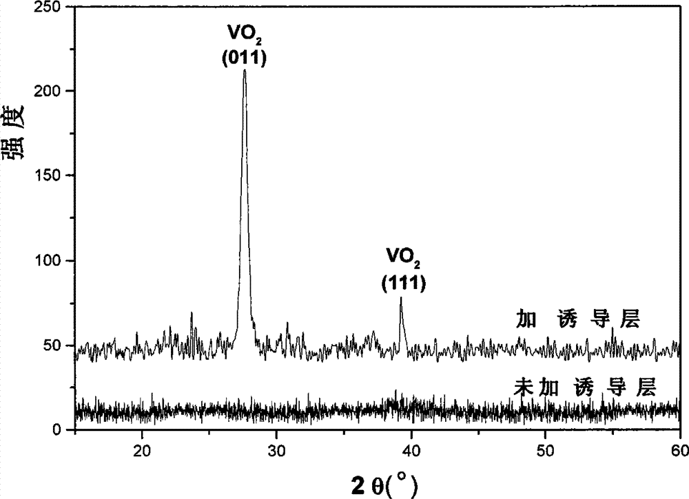
[0030] (1) Preparation of crystallization-inducing layer on glass surface

[0031] After the glass is routinely cleaned, a 5-20nm thick Ti or Si elemental film is sputtered and deposited on the glass surface by ion beam sputtering as a crystallization induction layer; or chemical vapor deposition is used on the cleaned glass surface ( PECVD) method deposits SiNx thin film of 40~80nm, as crystallization induction layer;

[0032] (2) Deposition of Vanadium Oxide Thin Film by DC Reactive Magnetron Sputtering

[0033] Using the DC reactive magnetron sputtering method, the vanadium oxide film is deposited on the crystallization induction layer by reactive sputtering; the reactive sputtering target is made of high-purity vanadium with a purity of 99.96% and doping elements with different atomic ratios; reactive sputtering Radiation sour...

Embodiment 1

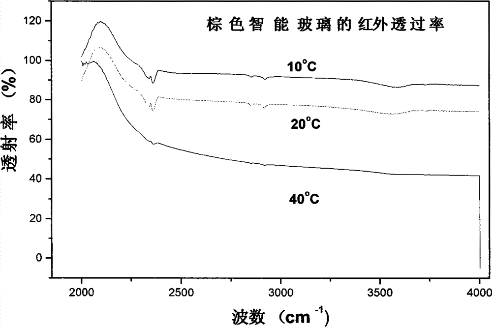
[0037] Embodiment 1 Brown smart glass preparation

[0038] 1. Preparation of crystallization-inducing layer on glass surface

[0039] After routine glass cleaning, chemical vapor deposition (PECVD) is used to deposit 70nm thick silicon-rich silicon nitride at 200°C as a crystallization induction layer, and its refractive index is 2.07;

[0040] 2. DC reactive magnetron sputtering vanadium oxide film deposition

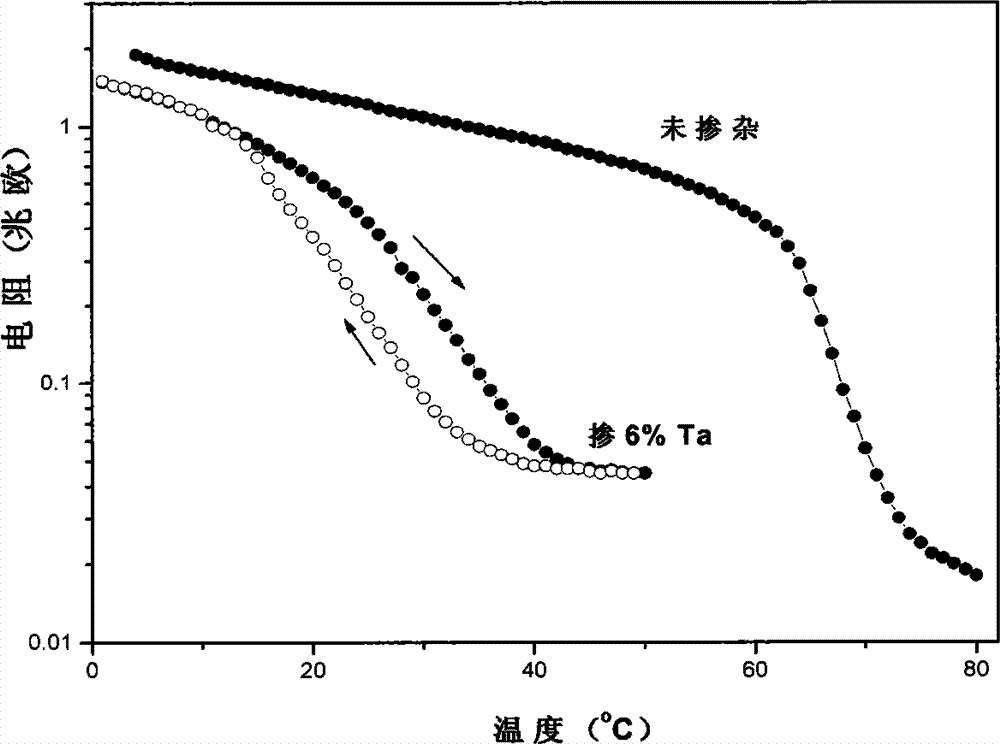
[0041] Using the DC reactive magnetron sputtering method, the vanadium oxide film was deposited on the crystallization induction layer by reactive sputtering; the reactive sputtering target was purchased 94% high-purity (99.96%) V and Ta with an atomic ratio of 6%. (purity 99.99%) molten alloy target. Reactive sputtering source gas is Ar / O 2 Mixed gas, Ar / O 2 The flow ratio is 8%, and the background vacuum of the sputtering chamber is 5×10 -4 Pa, the working vacuum degree during sputtering is 0.5Pa. During sputtering, a negative bias of 200V was applied to the sa...

Embodiment 2

[0045] Example 2 Preparation of blue smart glass

[0046] 1. Preparation of crystallization-inducing layer on glass surface

[0047] After the glass is routinely cleaned, use the ion beam sputtering method to deposit Ti with a purity of 99.99% on the glass surface with Ar ion sputtering, the sputtering acceleration voltage is 1500V, and the ion beam density is 0.4mA / cm 2 , the working vacuum degree is 1Pa, the sputtering deposition time is 5 minutes, and the thickness of the deposited Ti crystallization induction layer is about 10nm.

[0048] 2. DC reactive magnetron sputtering vanadium oxide film deposition

[0049] A direct current reactive magnetron sputtering method is used to deposit a vanadium oxide film on the crystallization induction layer by reactive sputtering; the deposited vanadium oxide film is a doped vanadium oxide film with a thickness of 180nm. The target material for reactive sputtering is a molten alloy target of 96% V (99.96% purity) and 1% La plus 3% Pd...


PUM

PropertyMeasurementUnit
phase transition temperatureaaaaaaaaaa
electrical resistanceaaaaaaaaaa
phase transition temperatureaaaaaaaaaa

Abstract

The invention relates to an industrial preparation method of smart glass capable of automatically regulating infrared transmittance. The industrial preparation method comprises the following steps: (1) conventionally cleaning glass, and then performing sputtering deposition of a Ti or Si elemental element film with the thickness of 5-20nm on the surface of the glass by an ion beam sputtering method as a crystallization inducing layer; (2) performing reactive sputtering deposition of a vanadium oxide film on the crystallization inducing layer by a direct current reactive magnetron sputtering method, wherein a reactive sputtering target is prepared by fusion of high-purity vanadium with the purity of 99.96% and doping elements with different atomic ratios; reactive sputtering source gas is Ar/O2 mixed gas, and the flow proportion of Ar/O2 is 5%-10%; and (3) performing heat treatment by adopting a fast heat treatment technology for heating by light of a halogen lamp after deposition of the vanadium oxide film, wherein the temperature in the whole heat treatment process is 450-550 DEG C, and the time is 10-20min; an annealing atmosphere adopts N2/O2 mixed gas, N2 and O2 are formed by gasification of liquid nitrogen and liquid oxygen, and the flow proportion of N2 to O2 is (98%-99%): (2%-1%).

Description

technical field [0001] The invention relates to the preparation technology of PVD deposition, doping, and coloring of smart thin films on glass, and in particular to an industrialized preparation method of smart glass with automatic infrared transmittance adjustment. Background technique [0002] Energy saving and environmental protection is a serious issue that the world must face today. In the hot summer, the direct radiation of 48% of the infrared rays (wavelength 0.78-2.5mm) in the sunlight to houses and cars is the main reason for the high temperature indoors and cars. Primary energy consumption. According to actual measurements, when the outdoor temperature is higher than 35°C, the indoor cooling temperature setting is lowered by 2°C, and the energy consumption of the air conditioner will be reduced by 20%. That's why there is an energy-saving slogan of "lowering the set temperature of the air conditioner by 1 degree". If you can try to reduce the indoor temperature...

Claims


Application Information

Patent Timeline
Patent Type & Authority Applications(China)
IPC IPC(8): C03C17/23C03C17/34
Inventor 李金华谢建生
Owner 李金华
Why Eureka
Try Eureka