Gallium-nitride-based enhancement type heterojunction field effect transistor with composite channel layer

A technology of heterojunction field effect and composite channel, which is applied in the direction of transistors, semiconductor devices, electrical components, etc., can solve the problems of material reliability influence, difficult realization of P-type GaN materials, high activation energy, etc., and achieve repeatability High, high maximum saturation leakage current, realize the effect of simple process

Active Publication Date: 2015-01-07
UNIV OF ELECTRONICS SCI & TECH OF CHINA
View PDF3 Cites 7 Cited by
  • Summary
  • Abstract
  • Description
  • Claims
  • Application Information

AI Technical Summary

Problems solved by technology

However, the P-type acceptor Mg activation energy of GaN materials is very high, and it is difficult to realize high-quality P-type GaN materials. At the same time, P-type doping will also affect the reliability of the material.

Method used


Image

  • Gallium-nitride-based enhancement type heterojunction field effect transistor with composite channel layer
  • Gallium-nitride-based enhancement type heterojunction field effect transistor with composite channel layer
  • Gallium-nitride-based enhancement type heterojunction field effect transistor with composite channel layer

Examples


Embodiment

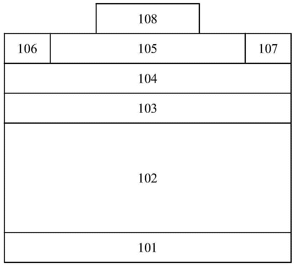
[0029] see figure 1 , is a structural schematic diagram of an existing GaN MIS-HFET device, which includes a substrate 101, an AlInGaN buffer layer 102, a GaN channel layer 103, an AlInGaN barrier layer 104, an insulating dielectric layer 105 and A source electrode 106, a drain electrode 107 formed on the AlInGaN barrier layer 104, and a gate 108 formed on the insulating dielectric layer 105, wherein the source electrode 106 and the drain electrode 107 form an ohmic contact with the AlInGaN barrier layer 104 , the gate 108 forms a Schottky contact with the insulating dielectric layer 105 .

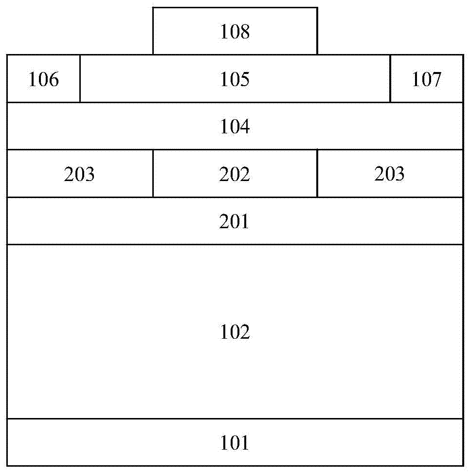
[0030] see figure 2 , is a schematic structural diagram of a gallium nitride-based enhancement heterojunction field effect transistor with a composite channel layer according to the present invention, which includes a substrate 101, an aluminum indium gallium nitrogen buffer layer 102, and an aluminum nitride back barrier layer 201 , a composite channel layer, an AlInGaN barrier layer 1...


PUM


Abstract

The invention relates to the technology of semiconductors, and provides a gallium-nitride-based enhancement type heterojunction field effect transistor with a composite channel layer. The problem that an existing gallium-nitride-based heterojunction field effect transistor is a depletion type component, but there is no relatively reliable enhancement type component is solved. According to the technical scheme, compared with an existing GaN MIS-HFET component, an aluminum nitride back barrier layer is arranged between an aluminum indium gallium nitrogen buffer layer and the channel layer of the gallium-nitride-based enhancement type heterojunction field effect transistor with the composite channel layer, and the channel layer is composite. The gallium-nitride-based enhancement type heterojunction field effect transistor with the composite channel layer has the advantages that reliability is improved, and repeatability is high.

Description

technical field [0001] The invention relates to semiconductor technology, in particular to gallium nitride (GaN)-based heterojunction field effect transistor strained N-channel metal oxide semiconductor field effect transistor (NMOSFET). Background technique [0002] Gallium nitride (GaN)-based heterojunction field effect transistor (HFET) has excellent characteristics such as large band gap, high critical breakdown electric field, high electron saturation velocity, good thermal conductivity, radiation resistance and good chemical stability. GaN materials can form two-dimensional electron gas heterojunction channels with high concentration and high mobility with materials such as aluminum gallium nitride (AlGaN), so they are especially suitable for high-voltage, high-power and high-temperature applications, and are the most suitable for power electronics applications. One of the most promising transistors. [0003] The conventional GaN HFET (gallium nitride-based heterojunc...

Claims


Application Information

Patent Timeline
Patent Type & Authority Applications(China)
IPC IPC(8): H01L29/778H01L29/06
CPCH01L29/1029H01L29/7783
Inventor 杜江锋潘沛霖陈南庭刘东于奇
Owner UNIV OF ELECTRONICS SCI & TECH OF CHINA
Why Eureka
Try Eureka