Nano vacuum triode with planar emitting cathode and manufacturing method thereof

A technology of vacuum triode and emitting cathode, which is applied in the direction of electron emitting electrode/cathode, cold cathode manufacturing, cold cathode, etc., and can solve the problems of signal quality reduction and energy loss

Active Publication Date: 2015-01-21
INST OF SEMICONDUCTORS - CHINESE ACAD OF SCI
View PDF3 Cites 16 Cited by
  • Summary
  • Abstract
  • Description
  • Claims
  • Application Information

AI Technical Summary

Problems solved by technology

For semiconductor devices commonly used today, electrons will be scattered by crystal lattices and i

Method used


Image

  • Nano vacuum triode with planar emitting cathode and manufacturing method thereof

Examples


Embodiment Construction

[0029] In order to make the object, technical solution and advantages of the present invention clearer, the present invention will be further described in detail below in conjunction with specific embodiments and with reference to the accompanying drawings.

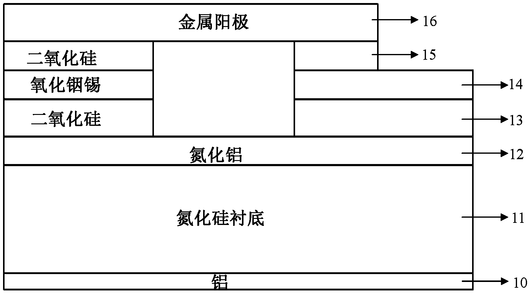
[0030] figure 1 A schematic structural view of a nanometer vacuum triode with a planar emitting cathode proposed by the present invention is shown. Such as figure 1 shown, which includes:

[0031] Substrate 11, which may be a conductive n-type silicon carbide (0001) substrate;

[0032] The back electrode 10, which is made on the back side of the substrate 11, can be made of metal aluminum;

[0033] Planar cold cathode 12, which is made on the front side of substrate 11, is formed by an aluminum nitride film with negative electron affinity;

[0034] The first insulating layer 13, which is made on the planar cold cathode 12, can be formed by silicon dioxide;

[0035] Indium tin oxide film gate layer 14, which is made o...


PUM


Abstract

The invention provides a nano vacuum triode with a planar emitting cathode and a manufacturing method of the nano vacuum triode with the planar emitting cathode. The method comprises the steps that a substrate, a back electrode, the planar cold cathode, a first insulation layer, a grid layer, a second insulation layer, a small cylindrical hole, a grid layer step and an anode layer are included; the back electrode is manufactured on the back face of the substrate; the planar cold cathode is manufactured on the front face of the substrate; the first insulation layer is manufactured on the planer cold cathode; the grid layer is manufactured on the first insulation layer; the second insulation layer is manufactured on the indium tin oxide thin film grid layer; the small cylindrical hole penetrates through the first insulation layer, the grid layer and the second insulation layer; the grid layer step is formed by etching the second insulation layer to the grid layer; the anode layer is manufactured on the second insulation layer; the total thickness of the first insulation layer, the indium tin oxide thin film grid layer and the second insulation layer ranges from 10 nanometers to 100 manometers. The defect that the electron emitting density of a tip structure is uneven, and a tip is prone to being damaged is overcome, and meanwhile the defect that the planar cathode needs higher threshold electric field intensity is overcome through the negative electron affinity characteristic of aluminum nitride materials.

Description

technical field [0001] The invention relates to the technical field of semiconductor devices and vacuum devices, in particular to a nanometer vacuum triode with a planar emitting cathode and a manufacturing method thereof. Background technique [0002] Vacuum does not contain substances that hinder the movement of electrons, so it is an ideal medium for electron conduction. For semiconductor devices that are commonly used today, electrons will be scattered by crystal lattices and ionized impurities during transport in the device, causing energy loss and degradation of signal quality. When electrons are transported in a vacuum, they will not be disturbed by these scattering effects. Therefore, compared with solid-state semiconductor devices, under the same conditions, vacuum tubes can work at higher frequencies and power conditions. In the history of scientific development, the replacement of vacuum devices by solid-state devices is not entirely due to performance reasons, b...

Claims


Application Information

Patent Timeline
IPC IPC(8): H01L29/73H01L29/43H01L21/33
CPCH01J9/025H01J19/24H01J21/10
Inventor 侍铭陈平赵德刚朱建军刘宗顺江德生
Owner INST OF SEMICONDUCTORS - CHINESE ACAD OF SCI
Why Eureka
Try Eureka