Field enhancement metal insulator-semiconductor/metal insulator-metal electronic emitter

A technology of electron emitters and insulators, applied in circuits, electrical components, cold cathodes of discharge tubes, etc., can solve problems such as high stability and high reliability difficulties

Inactive Publication Date: 2003-04-23
HEWLETT PACKARD CO
View PDF2 Cites 10 Cited by
  • Summary
  • Abstract
  • Description
  • Claims
  • Application Information

AI Technical Summary

Problems solved by technology

[0007] In other words, with previous electron emitters, it was very difficult to achieve high current density, high stability, and high reliability in one device

Method used


Image

  • Field enhancement metal insulator-semiconductor/metal insulator-metal electronic emitter
  • Field enhancement metal insulator-semiconductor/metal insulator-metal electronic emitter
  • Field enhancement metal insulator-semiconductor/metal insulator-metal electronic emitter

Examples


Embodiment Construction

[0020] For simplicity and purpose of illustration, the principles of the invention are described primarily in terms of exemplary embodiments. However, those of ordinary skill in the art will appreciate that these principles are equally applicable to various types of electron emitters.

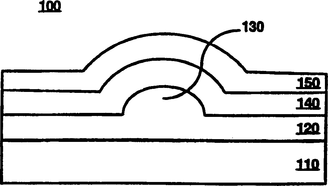
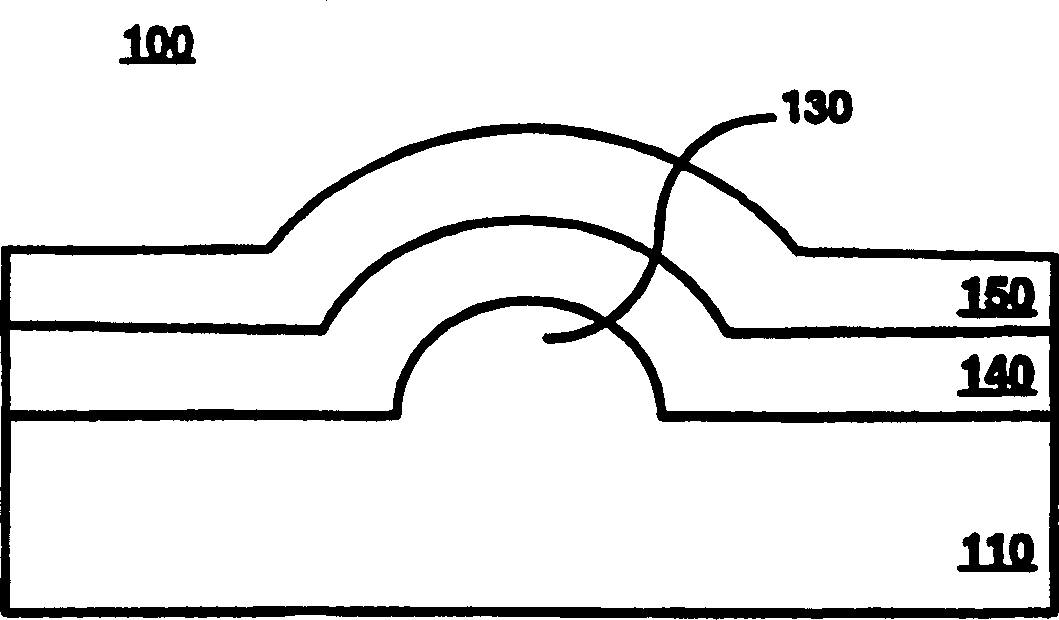
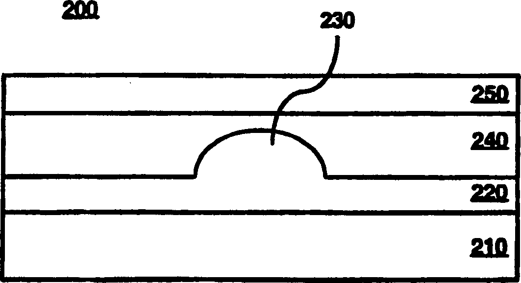
[0021] Figure 1A and 1B Cross-sectional views of first and second embodiments of an exemplary FEMIS electron emitter in an aspect of the invention are shown. As shown, the electron emitter 100 may include a conductive substrate 110 . The conductive substrate 110 can be made of metal (aluminum, tungsten, titanium, copper, gold, tantalum, platinum, iridium, palladium, cerbium, chromium, magnesium, scandium, yttrium, vanadium, pickaxe, niobium, molybdenum, silicon, beryllium, hafnium, silver, osmium and any alloy, and their multilayer films); doped polysilicon; doped silicon; graphite; metal coated glass, ceramics or plastics; indium tin oxide (ITO) coated glass, ceramics or plastics, etc. And...


PUM


Abstract

In an electron emitter based on Metal-Insulator-Semiconductor or Metal-Insulator-Metal emitters, field emission structures are enclosed within the emitter structure. The electron emitter may include a conductive substrate and an electron supply layer formed on the conductive substrate. The electron supply layer, for example undoped polysilicon, has protrusions formed on its surface. The sharpness and density of protrusions may be controlled. Above the electron supply layer and the protrusions, an insulator may be formed thereby enclosing the protrusions. A top conductive layer may be formed above the insulator. The enclosed protrusions are relatively insensitive to vacuum contamination.

Description

field of invention [0001] Generally, the present invention relates to electron emitters. In particular, the present invention relates to field-enhanced metal-insulator-semiconductor (MIS) or metal-insulator-metal (MIM) electron emitters, hereinafter collectively referred to as FEMIS. Background of the invention [0002] Electron emission technology today takes many forms. For example, cathode ray tubes (CRTs) play a major role in such devices as televisions and computer monitors. Electron emission technology plays a key role in X-ray machines and electron microscopes. Additionally, microscopic cold cathodes can be used in e-beam lithography, for example, in the fabrication of integrated circuits, information storage devices of the kind described in US Patent No. 5,557,596 to Gibson et al., electronic amplifiers, and flat panel displays. Actual requirements for electron emission depend on the specifics of a particular application. But in general, for all applications, the...

Claims


Application Information

Patent Timeline
Patent Type & Authority Applications(China)
IPC IPC(8): H01J1/312
CPCB82Y10/00H01J1/312
Inventor X·圣H·比雷基S·T·林H·P·郭S·L·纳伯惠斯
Owner HEWLETT PACKARD CO
Why Eureka
Try Eureka