Preparation method of gallium nitride nanowires
A technology of gallium nitride nanowires and gallium sources, which is applied in nanotechnology, nanotechnology, nitrogen-metal/silicon/boron binary compounds, etc., can solve the problem of affecting the quality of GaN nanowires, insufficient mixing of gallium sources, gallium source Difficult to weigh and other problems, to avoid the problem of not easy to grind fully or difficult to weigh, the preparation process is simple and easy, and the production cost is low.
- Summary
- Abstract
- Description
- Claims
- Application Information
AI Technical Summary
Problems solved by technology
Method used
Image
Examples
Embodiment 1
[0037] A preparation method of gallium nitride nanowires, specifically comprising the following steps:
[0038] (1), preparation of mixed gallium source;
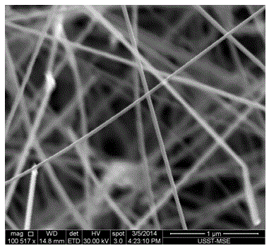
[0039] GaN with a purity of 99.999% and Ga with a purity of 99.999% 2 o 3 According to mass ratio Ga 2 o 3 : GaN is mixed and ground at 2:1 to obtain a mixed gallium source with a particle size of 700-900nm and a length of about 2μm;
[0040] (2) Growth of gallium nitride nanowires
[0041] Put the mixed gallium source in step (1) into a small porcelain boat, put the Si substrate material coated with a catalyst Ni layer into a quartz glass tube, then put the small porcelain boat into the quartz glass tube, and ensure that the mixed gallium The distance between the center of the source and the center of the Si substrate material coated with the catalyst Ni layer is 11cm, then put the quartz glass tube into the tube furnace, and align the small porcelain boat with the center of the tube furnace;
[004...
Embodiment 2
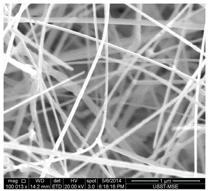
[0056] Just replace the Si substrate material coated with the catalyst Ni layer in step (2) with the Si substrate material coated with the catalyst Au layer, and other conditions remain the same. The light yellow substance obtained on the surface of the substrate material is gallium nitride nanowire;
[0057] The Si substrate material coated with a catalyst Au layer described in the above step (2), that is, the Si substrate material coated with a catalyst Au layer with a thickness of 3nm in the orientation (100) direction;
[0058] The catalyst Au layer coated in the orientation (100) direction is prepared by electron beam evaporation in the orientation (100) direction of the Si substrate material, and its preparation process specifically includes the following steps:
[0059] Using pure metal Ni as the evaporation source, an electron beam evaporation method is used to electrodeposit a layer of Au on the Si substrate material oriented in the (100) direction to obtain a Si subs...
Embodiment 3
[0064] Just change the center of the mixed gallium source in step (2) and the center of the Si substrate material coated with the catalyst Ni layer to 10cm, and other conditions remain unchanged, the same as in Example 1, and finally the Si substrate material coated with the catalyst Ni layer The light yellow substance obtained on the surface of the GaN nanowire is GaN.
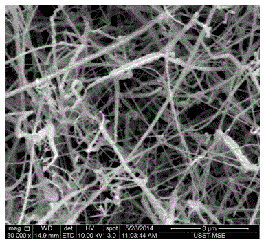
[0065] Quanta FEG is used to scan the gallium nitride nanowires obtained above, and the obtained scanning electron microscope picture is as follows Figure 5 shown, from Figure 5 It can be seen that the distribution of GaN nanowires is sparse, the thickness is uneven, the growth is disordered, and a sheet-like structure appears.
PUM
| Property | Measurement | Unit |
|---|---|---|
| Particle size | aaaaa | aaaaa |
| Length | aaaaa | aaaaa |
| Diameter | aaaaa | aaaaa |
Abstract
Description
Claims
Application Information


