Intermittent-annealing isothermal-growth multi-quantum well LED extension structure and manufacturing method thereof

A multi-quantum well and epitaxial structure technology, applied in electrical components, circuits, semiconductor devices, etc., can solve the problems of ineffective formation of electron holes, high quantum barrier dislocation density, affecting luminous efficiency, etc., to save heating and cooling time. , the crystal plane orientation is unified, and the production capacity is obviously improved.

Inactive Publication Date: 2015-01-28
SUZHOU NANOJOIN PHOTONICS
View PDF9 Cites 10 Cited by
  • Summary
  • Abstract
  • Description
  • Claims
  • Application Information

AI Technical Summary

Problems solved by technology

This contradiction is one of the main bottlenecks restricting the development of GaN-based LED epitaxial technology. At the same time, in this growth mode, due to the need to continuously switch between high and low growth temperatures, a large amount of temperature Ramp is required, resulting in the current LED industry. Overall low; considering that in the entire epitaxial process of MOCVD epitaxial growth LED, the MQW growth time accounts for half of the total epitaxial wafer growth time, so how to shorten the MQW growth time and obtain high-quality barrier materials has become an important issue for improving GaN-based LED epitaxy. A major factor in wafer production efficiency
[0005] Under the current process conditions, growing multiple quantum wells at the same temperature cannot meet the structural design requirements for high-quality quantum barriers. The quantum barriers formed have a high dislocation density and cannot effectively form an effective barrier for electron-hole pairs, which affects the luminous efficiency.

Method used


Image

  • Intermittent-annealing isothermal-growth multi-quantum well LED extension structure and manufacturing method thereof
  • Intermittent-annealing isothermal-growth multi-quantum well LED extension structure and manufacturing method thereof
  • Intermittent-annealing isothermal-growth multi-quantum well LED extension structure and manufacturing method thereof

Examples


Embodiment Construction

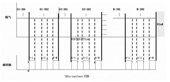
[0038] The invention provides a discontinuous annealing and same-temperature growth multi-quantum well LED epitaxial structure and a manufacturing method. The method adopts MOCVD equipment of Aixtron Company for epitaxial growth, and uses NH 3 , TMGa / TEGa, and TMIn are respectively used as N, Ga, and In sources.

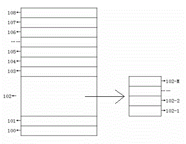
[0039] A multi-quantum well LED epitaxial structure grown at the same temperature by intermittent annealing, including a substrate on which a buffer layer, an n-GaN layer, an MQW active layer, p-GaN and a p-type contact layer are sequentially grown , the MQW active layer includes at least two multi-quantum well layers, generally 5-20, and 15 are grown in this embodiment. The multi-quantum well layer includes an InGaN quantum well layer, a GaN protection layer and a GaN quantum barrier layer from bottom to top, and the GaN quantum barrier layer consists of at least one GaN quantum barrier thin layer and a quantum barrier annealed layer grown at intervals. Generally, ...


PUM

PropertyMeasurementUnit
thicknessaaaaaaaaaa

Abstract

The invention discloses a manufacturing method of an intermittent-annealing isothermal-growth multi-quantum well LED (light-emitting diode) extension structure, and the manufacturing method comprises the following steps of: preparing a substrate, and treating it at high temperature under hydrogen atmosphere; successively growing a buffer layer and a n-GaN layer on the treated substrate surface; periodically growing a MQW (multiple quantum well) active layer on the n-GaN layer; successively growing a p-GaN contact layer and a P-type contact layer on the MQW active layer; the MQW active layer is composed of at least two MQW layers, each MQW layer includes an InGaN MQW layer, a GaN protection layer and a GaN quantum barrier layer, and each MQW layer is grown at the same temperature. In the manufacturing method, through intermediate intermittent annealing, the extension structure has more uniform crystal orientation and higher crystal lattice quality; through the method, a high-quality MQW structure layer can be manufactured, the luminous efficiency is improved by more than 10%, much original heating and cooling time is saved in the MQW and the capacity is also obviously increased. The surface of low-temperature GaN material is smoothed to achieve uniform two-dimensional growth of the barrier so as to obtain a high-quality MQW material.

Description

technical field [0001] The invention belongs to the field of LED epitaxial technology growth, and in particular relates to a multi-quantum well LED epitaxial structure and a manufacturing method for multiple intermittent annealing and recrystallization growth. Background technique [0002] LED has now entered the stage of commercial production. How to further shorten the growth time of epitaxial wafers to increase production capacity under the premise of obtaining high-quality epitaxial wafers has become a focus of the industry. [0003] At present, MOCVD is used for the commercial production of epitaxial wafers. However, due to the difference in the temperature atmosphere for the growth of InGaN quantum wells and GaN quantum barriers, the InGaN quantum well layer can be grown in a high temperature environment and H 2 In the growth atmosphere, In is easy to precipitate and dissociate, and cannot effectively form devices and quantum well layers, while the GaN quantum barrier ...

Claims


Application Information

Patent Timeline
Patent Type & Authority Applications(China)
IPC IPC(8): H01L33/06H01L33/14H01L33/00
CPCH01L33/005H01L33/06H01L33/14H01L2933/0008
Inventor 南琦王怀兵王辉吴岳傅华
Owner SUZHOU NANOJOIN PHOTONICS
Why Eureka
Try Eureka