Perovskite solar cell with conducting polymer as back electrode and preparing method of perovskite solar cell
A technology of conductive polymers and solar cells, applied in the field of solar cells, can solve problems such as complex processes, and achieve the effects of simple processes, easy mass production, and low manufacturing costs
- Summary
- Abstract
- Description
- Claims
- Application Information
AI Technical Summary
Problems solved by technology
Method used
Image
Examples
Embodiment 1
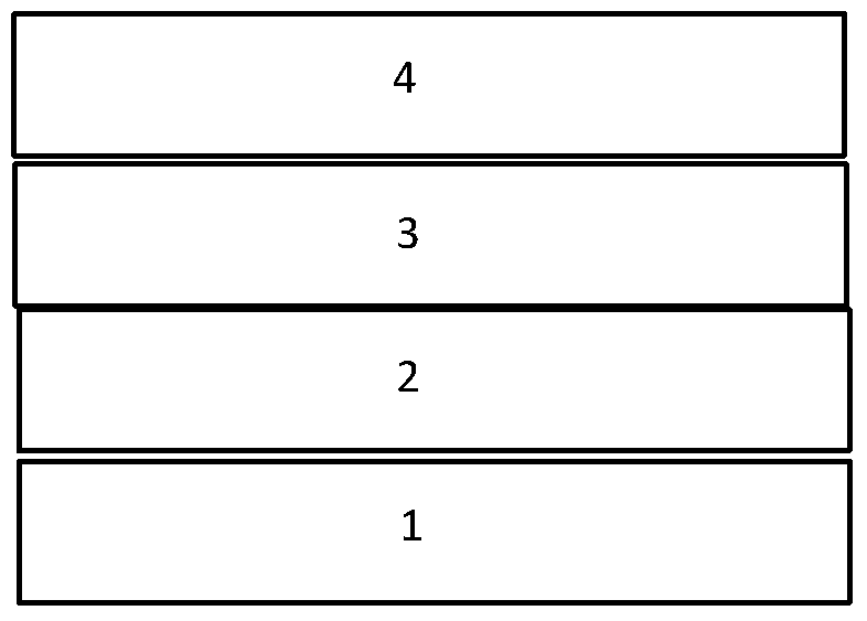
[0025] A perovskite solar cell with a conductive polymer as the back electrode, such as figure 1 As shown, it consists of a transparent conductive glass substrate 1, an isoelectron transport layer 2, a light-absorbing perovskite material layer 3, and a conductive polymer back electrode layer 4, and sequentially forms a laminated structure. The transparent conductive glass substrate 1 is ITO conductive glass with a thickness of 100nm; the isoelectron transport layer 2 is a sputtered ZnO film with a thickness of 40nm; the light-absorbing perovskite material layer 3 is CH 3 NH 3 PB 3 layer with a thickness of 300 nm; the back electrode layer 4 is a polyaniline film with a thickness of 20 nm.
Embodiment 2
[0027] A perovskite solar cell with a conductive polymer as the back electrode, which is composed of a transparent conductive glass substrate, an isoelectron transport layer, a light-absorbing perovskite material layer, and a conductive polymer back electrode layer to form a laminated structure in sequence, The transparent conductive glass substrate is FTO conductive glass with a thickness of 350nm; the other electron transport layer is TiO obtained by spin coating 2 thin film with a thickness of 60nm; the light-absorbing perovskite material layer is CH 3 NH 3 SnBr 3 layer with a thickness of 400nm; the back electrode layer is a polyaniline film with a thickness of 100nm. Example 3:
Embodiment 3
[0028] A perovskite solar cell with a conductive polymer as the back electrode, such as figure 1 As shown, it consists of a transparent conductive glass substrate, an isoelectron transport layer, a light-absorbing perovskite material layer, and a conductive polymer back electrode layer, and sequentially forms a laminated structure. The transparent conductive glass substrate is FTO conductive glass, with a thickness of 1000nm; ETC layer is sputtered TiO 2 thin film with a thickness of 20nm; the light-absorbing perovskite material layer is C 4 h 9 NH 3 PB 2 The Cl layer has a thickness of 300nm; the back electrode layer is a polyaniline film with a thickness of 100nm.
PUM
 Abstract
Description
Claims
Application Information
