
Light control chip based on electric control liquid crystal dual-mode micro lens

A micro-lens and optical chip technology, applied in optics, nonlinear optics, instruments, etc., can solve the problem of uneven spectral transmittance of film alloy electrode materials, loss of electric control dielectric ability of liquid crystal molecules, and influence on the construction efficiency of space electric field, etc. problems, to achieve excellent electrical and electro-optical control capabilities, optical conversion performance, high light transmission and thermal conductivity performance, and long-lasting effects of liquid crystal electrical properties

Active Publication Date: 2015-02-04
HUAZHONG UNIV OF SCI & TECH
View PDF5 Cites 3 Cited by
  • Summary
  • Abstract
  • Description
  • Claims
  • Application Information

AI Technical Summary

Problems solved by technology

The defects of the above-mentioned typical structure mainly include: (1) The transmittance of light waves is generally about 85%, and for higher transmittance requirements, an additional anti-reflection film system is required; (2) The film alloy electrode material has spectral transmission (3) Carriers in the alloy material, such as cations and electrons, sometimes penetrate the initial alignment layer of the liquid crystal and penetrate into the liquid crystal In the material, by neutralizing the polar groups of the liquid crystal molecules, the liquid crystal molecules lose the ability to control the dielectric, thereby significantly reducing the light control efficiency and significantly shortening the life of the device; (4) Due to the large resistance of the metal material, its thermal effect And the skin effect under the control of higher frequency electromagnetic signals will seriously affect the construction efficiency of the space electric field applied in the liquid crystal material, thereby significantly reducing the light control ability of the device

Method used

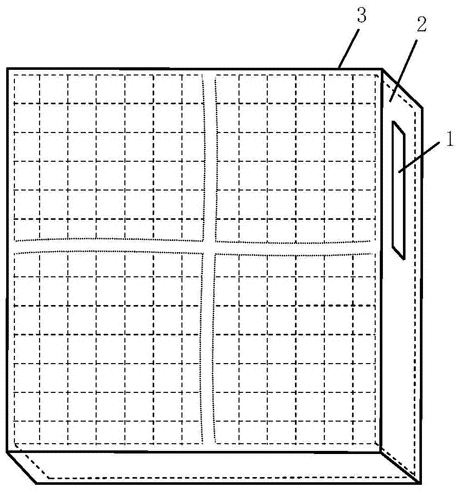

Image

  • Light control chip based on electric control liquid crystal dual-mode micro lens
  • Light control chip based on electric control liquid crystal dual-mode micro lens
  • Light control chip based on electric control liquid crystal dual-mode micro lens

Examples


Embodiment Construction

[0021] In order to make the object, technical solution and advantages of the present invention clearer, the present invention will be further described in detail below in conjunction with the accompanying drawings and embodiments. It should be understood that the specific embodiments described here are only used to explain the present invention, not to limit the present invention. In addition, the technical features involved in the various embodiments of the present invention described below can be combined with each other as long as they do not constitute a conflict with each other.

[0022] In recent years, graphene technology has developed by leaps and bounds, and several outstanding properties displayed have brought dawn to the development of a new generation of electronically controlled liquid crystal microlens technology. Its typical features include: super-strong electrical conductivity, super-high light transmittance (~>97%), currently the material with the highest ele...


PUM

PropertyMeasurementUnit
porosityaaaaaaaaaa

Abstract

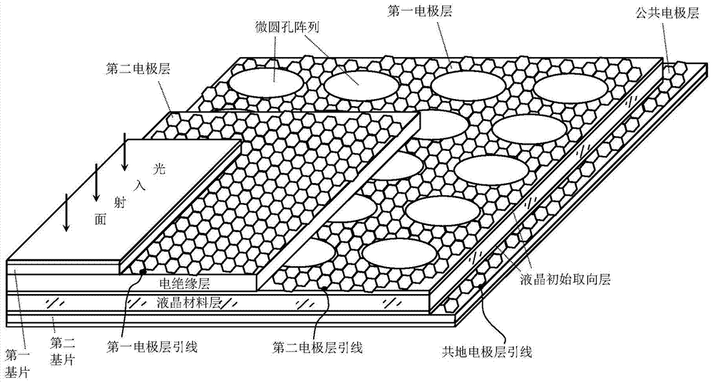
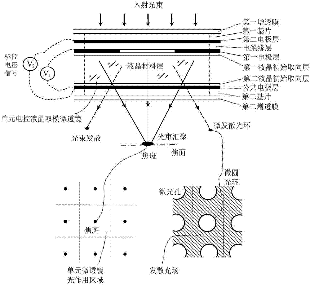
The invention discloses a light control chip based on an electric control liquid crystal dual-mode micro lens. The chip comprises an area array electric control liquid crystal dual-mode micro lens, wherein the area array electric control liquid crystal dual-mode micro lens comprises: a liquid crystal material layer; a first liquid crystal initial orientation layer, a first electrode layer, an electric insulation layer, a second electrode layer, a first substrate and a first antireflection film which are sequentially arranged on the upper surface of the liquid crystal material layer; and a second liquid crystal initial orientation layer, a common electrode layer, a second substrate and a second antireflection film which are sequentially arranged on the lower surface of the liquid crystal material layer. The first electrode layer is formed by a homogenization graphene film; circular holes in m*n-element array distribution are formed on the homogenization graphene film; each of the common electrode layer and the second electrode layer is formed by a homogenization graphene film which is homogeneous with the first electrode layer. The chip is capable of carrying out the operation of collecting array light or diverging and transforming light of wave beams, and has the characteristics of being high in optical wave beam modulation capability, excellent in electro-optical performance, high in environmental adaptability and easy to match with other optical and optoelectronic mechanical structures.

Description

technical field [0001] The invention belongs to the technical field of optical beam precision measurement and control, and more specifically relates to a light control chip based on an electronically controlled liquid crystal dual-mode microlens. Background technique [0002] In recent years, the electronically controlled liquid crystal microlens technology has developed rapidly, and has shown strong electric focusing, electric swing focus, electric control wave front, electric point spread function, electric depth of focus, electric gating aperture, electric Energy efficiency characteristics such as adjusting the photosensitive field of view, electrically switching the light convergence and light divergence mode, and electrically adjusting the beam divergence shape and degree. The time constant between the stable light-controlling states of liquid crystal materials is currently as low as sub-milliseconds, and the laboratory level is as low as microseconds. The light contro...

Claims


Application Information

Patent Timeline
Patent Type & Authority Applications(China)
IPC IPC(8): G02F1/1343G02F1/133G02F1/29G01J3/12
CPCG02F1/13306G02F1/13439G02F1/29
Inventor 张新宇罗俊佟庆雷宇桑红石谢长生
Owner HUAZHONG UNIV OF SCI & TECH
Learn More