
Silicon nitride anti-reflection film for crystalline silicon solar cell and preparation method thereof

A solar cell, silicon nitride reduction technology, applied in the direction of circuits, photovoltaic power generation, electrical components, etc., can solve the problem that the photoelectric conversion efficiency cannot achieve the maximum improvement, the film layer design cannot achieve the anti-reflection efficiency, and special gas multi-process Process and other issues, to achieve the effect of facilitating large-scale commercial production, improving cell efficiency, and simple process

Active Publication Date: 2016-08-31
九州方园新能源股份有限公司
View PDF6 Cites 0 Cited by
  • Summary
  • Abstract
  • Description
  • Claims
  • Application Information

AI Technical Summary

Problems solved by technology

At present, the mainstream solar cell coating process is single-layer coating or double-layer coating, and there are also some technical methods for multi-layer coating. For example, the patent 201210401694.0 process has more special gases, and the process is more complicated. The manufacturing cost is higher and it cannot be commercialized on a large scale. Production, and the design of the film layer cannot achieve the optimal anti-reflection efficiency, and the final photoelectric conversion efficiency cannot achieve the maximum improvement

Method used


Image

  • Silicon nitride anti-reflection film for crystalline silicon solar cell and preparation method thereof

Examples


Embodiment 1

[0025] A method for preparing a silicon nitride antireflection film for a crystalline silicon solar cell, comprising the steps of:

[0026] 1) Clean the silicon substrate after phosphorus diffusion to ensure that the surface of the silicon wafer has good hydrophobicity and is clean and free of water stains.

[0027] 2) Insert the cleaned silicon substrate into the graphite boat according to the conventional method, put it into the quartz tube of the PECVD equipment, then vacuumize the quartz tube and raise the temperature to 450°C, and keep the temperature at 480S.

[0028] 3) When the equipment is evacuated below 10 mttor, inject 5800 SCCM of NH into the quartz tube after evacuation of the PECVD equipment 3 Gas, and keep the pressure in the quartz tube at 1800 mttor, keep the constant pressure for 1-2min, set the power of the high frequency power supply to 6000W, turn on the high frequency power supply, and keep the NH 3 The flow rate of the gas is constant, and the NH3 T...


PUM

PropertyMeasurementUnit
thicknessaaaaaaaaaa
thicknessaaaaaaaaaa
thicknessaaaaaaaaaa

Abstract

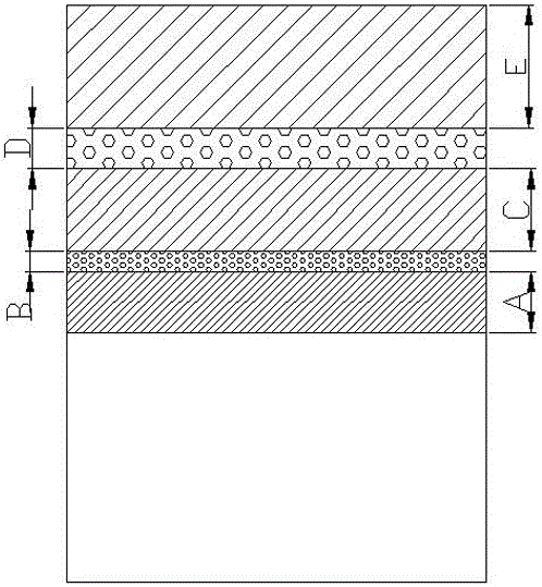
The invention discloses a silicon nitride anti-reflection film which uses three gases of N2, NH3 and SiH4 to coat a crystalline silicon solar cell with multi-layer interlaced changes under high-frequency electric shock, and belongs to the field of crystalline silicon solar cells. The invention comprises a silicon nitride anti-reflection film deposited on a silicon chip with alternately varying refractive index and film thickness. The refractive index is first small and then large, but the N value of the odd-numbered film layers decreases sequentially, and the N value of the even-numbered film layers also decreases sequentially. The film thickness is first thicker and then thinner (single-numbered film thickness, even-numbered film layer is thinner), and the value of the film thickness result of the process is inversely proportional to the refractive index value, that is, the number of single films is compared with the number of double-layer films. It will get thicker and thicker. According to the physical characteristics of the multi-layer anti-reflection film, the destructive interference of the alternating anti-reflection film has better transmittance, increases the absorption of light, and then generates more photogenerated electrons at the P / N junction, improving the photoelectric conversion efficiency .

Description

technical field [0001] The invention relates to a multilayer staggered gradient silicon nitride anti-reflection film for a crystal solar cell, which has good surface passivation effect and anti-reflection effect, and can improve the photoelectric carrier quantity and conversion efficiency of the solar cell. The invention belongs to the field of crystalline silicon solar cells. Background technique [0002] The production process of traditional solar cells includes: texturing, diffusion, etching, PSG removal, anti-reflection coating, screen printing, and sintering. Among them, anti-reflection coating is an important link to reduce sunlight reflection and passivate the wafer surface to improve the minority carrier lifetime. At present, the mainstream solar cell coating process is single-layer coating or double-layer coating, and there are also some technical methods for multi-layer coating. For example, the patent 201210401694.0 process has more special gases, and the proce...

Claims


Application Information

Patent Timeline
Patent Type & Authority Patents(China)
IPC IPC(8): H01L31/0216H01L31/18C23C16/34C23C16/503C23C16/52
CPCB32B5/145B32B5/147B32B9/00C23C16/345C23C16/503C23C16/52H01L31/02167H01L31/18Y02E10/50Y02P70/50
Inventor 傅强董道宴张崇超刘代军陈红玉匡英汪双
Owner 九州方园新能源股份有限公司
Learn More