Method for cleaning passivated GaAs wafer surface

A wafer, ozone technology, applied in electrical components, semiconductor/solid state device manufacturing, circuits, etc., can solve problems such as environmental hazards and GaAS surface defects

Inactive Publication Date: 2015-03-04
BEIJING UNIV OF TECH
View PDF1 Cites 6 Cited by
  • Summary
  • Abstract
  • Description
  • Claims
  • Application Information

AI Technical Summary

Problems solved by technology

However, the S passivation method has certain hazards to the environment, and there are certain defects on the GaAS surface after treatment.

Method used


Image

  • Method for cleaning passivated GaAs wafer surface

Examples


Embodiment

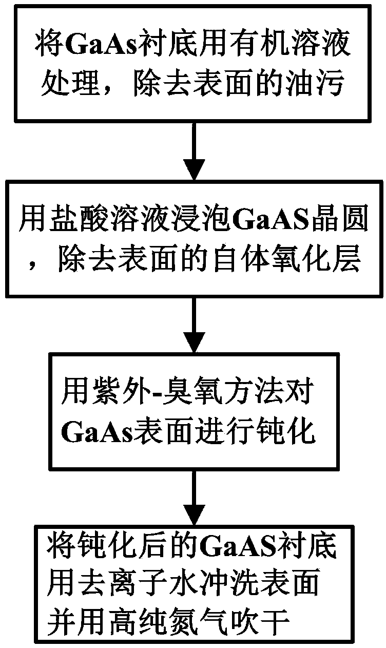
[0019] According to the method, HCl is used to remove the autogenous oxide layer on the surface of the wafer and the UV-ozone method is used for passivation.

[0020] Table 1 is the comprehensive XPS spectrum data of the wafer treated by this method, from which it can be seen that the chemical dose ratio of the surface after treatment is also close to that of the bulk, that is, this method will not affect the surface characteristics of the wafer while completing the passivation.

[0021] 2. The low-noise device and power device were prepared by four ion-implanted materials with different passivation, and the noise and power performance were measured at 4GHz and 12GHz, and the antistatic ability was tested.

[0022] Table 2 shows the comparison results of power and antistatic ability between this method and the other two methods. Among them, Table 2(a) is the test result of the die working at 4GHz, and Table 2(b) is the test result of the die It is the result of testing under 1...


PUM


Abstract

The invention relates to a method for cleaning a passivated GaAs wafer surface. According to the method, A GaAs wafer is processed by an organic solution to remove the surface oil contamination; a GaAs substrate is soaked by a hydrochloric acid solution to remove a surface oxidation layer; the GaAs surface is passivated by using an ultraviolet-ozone method; and deionized water is used for washing the surface of the passivated GaAs substrate and drying is carried out by using high-purity nitrogen. Therefore, the surface oxide of the processed wafer is closed to the surface characteristic of the wafer before processing; and the power characteristic, the gain characteristic, and especially the voltage withstanding characteristic of the device after passivation are substantially improved.

Description

technical field [0001] The invention relates to a preparation process of a GaAS-based microwave device, in particular to a method for cleaning and passivating the surface of a GaAS wafer during the preparation process. Background technique [0002] GaAs has the advantages of high electron mobility, large band gap, and lower power consumption than si, and has become one of the preferred materials for high-performance microelectronics and optoelectronic semiconductor devices. However, the surface of GaAs is easily oxidized, forming a high Density of states at the surface and interface, thereby giving rise to Fermi level pinning and high surface recombination velocities. Moreover, its own oxide layer has a loose structure, poor component stability, and no passivation function at all. [0003] The development of an effective surface passivation (Surface Passivation) method has become an extremely important and key step in the development of GaAS-based microwave devices. Studie...

Claims


Application Information

Patent Timeline
Patent Type & Authority Applications(China)
IPC IPC(8): H01L21/02
CPCH01L21/0201H01L21/02054
Inventor 王智勇张绵王青尧舜高鹏坤郑建华
Owner BEIJING UNIV OF TECH
Why Eureka
Try Eureka