Method for manufacturing polymer PMMA optical waveguide device based on electric printing technology

A polymer, electro-printing technology, used in optical waveguides, light guides, optical components, etc., can solve problems such as high prices

Active Publication Date: 2015-03-25
长春市华信科瑞光电技术有限公司
View PDF3 Cites 10 Cited by
  • Summary
  • Abstract
  • Description
  • Claims
  • Application Information

AI Technical Summary

Problems solved by technology

However, these preparation technologies are relatively expensive, and often include many complicated process steps in the preparation pro

Method used


Image

  • Method for manufacturing polymer PMMA optical waveguide device based on electric printing technology
  • Method for manufacturing polymer PMMA optical waveguide device based on electric printing technology
  • Method for manufacturing polymer PMMA optical waveguide device based on electric printing technology

Examples


Embodiment 1

[0062] Embodiment 1: Preparation and Refractive Index Characterization of PMMA Core Material

[0063] The core material used in the present invention is a polymer—polymethyl methacrylate, which can be prepared by copolymerizing methyl methacrylate, and the prepared material has high transparency and good film-forming properties. , low price and easy synthesis, etc., are widely used in polymer planar optical waveguide devices. Its molecular structural formula is shown in general formula (I).

[0064]

[0065] The obtained PMMA material was spin-coated on a cleaned Si substrate (a total of 4 samples) by a spin-coating process, and then the spin-coated polymer film was placed in a vacuum oven for low-temperature curing (30 ° C) for 2.5 hours. Remove the solvent from the film. Next, 4 identical samples were cured at curing temperatures of 30°C, 60°C, 90°C, 120°C, 150°C and 180°C for 2 hours respectively, and the refractive index of the material was measured with an ellipsomet...

Embodiment 2

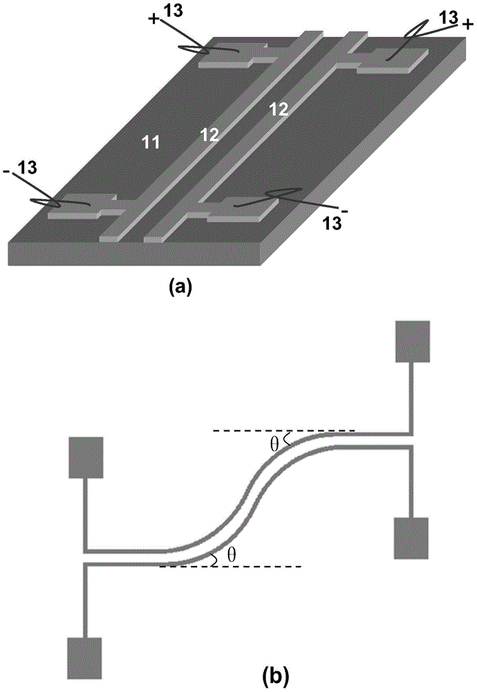
[0066] Embodiment 2: prepare electroprinting template on PMMA substrate

[0067] First, clean the PMMA substrate. A PMMA substrate (thickness 2 mm) with low price and low thermal conductivity was selected as the substrate of the electroprinting template, which was repeatedly wiped with acetone and ethanol cotton balls in sequence, rinsed with deionized water, and finally dried with nitrogen .

[0068] Then, integrated electrode wiring is prepared. A layer of aluminum film with a thickness of 300nm was evaporated on the cleaned PMMA substrate by evaporation process, and then a layer of BP212 positive photoresist with a thickness of 2 μm was spin-coated on the aluminum film by spin coating process. Pre-bake for 20 minutes at ℃; then, on the photolithography machine, put it in close contact with the electrode mask plate (chrome plate) complementary to the waveguide to carry out the photolithography of the plate. The exposure time of the photoresist is 7 seconds, and the mask is...

Embodiment 3

[0070] Example 3: Using electroprinting technology on SiO 2 Preparation of Polymer PMMA Optical Waveguide on Substrate

[0071] First, a layer of SiO with a thickness of 3 μm is grown on the silicon substrate 2 Lower confinement layer (lower cladding). In order to suppress the leakage of the light field into the silicon substrate with a higher refractive index, a thicker layer of SiO needs to be grown on the silicon wafer. 2 The lower confinement layer is used as the lower cladding layer of the waveguide, and the method of dry oxygen oxidation and wet oxygen oxidation is used to grow SiO 2 layer, the oxidation temperature was kept at 1200°C, dry oxygen oxidation was performed for 30 minutes first, then wet oxygen oxidation and dry oxygen oxidation were alternately carried out 6 times, among which wet oxygen oxidation was 60 minutes, dry oxygen oxidation was 30 minutes, and finally dry oxygen oxidation was 30 minutes , and finally a silicon dioxide lower cladding layer with ...


PUM

PropertyMeasurementUnit
Thicknessaaaaaaaaaa
Sizeaaaaaaaaaa
Thicknessaaaaaaaaaa

Abstract

The invention relates to a method for manufacturing a polymer PMMA optical waveguide device based on an electric printing technology and belongs to the field of manufacturing technologies of polymer planar optical waveguide devices. The method comprises the steps that a PMMA substrate is coated with an evaporation aluminum film; afterwards, integrated electrode wires of different widths from a few microns to dozens of microns are manufactured based on semiconductor technologies of spin coating, photoetching, wet etching and the like, and then an electric printing template is manufactured; next, a thin polymer film is heated through the electric printing template, so that the refractive index of a polymer material changes, and then the integrated optical circuit device is manufactured. According to the device and the method for manufacturing the device, the device is low in cost and high in yield, the technologies are simple, the manufacturing speed is high, and therefore the device and the manufacturing method are suitable for mass production.

Description

technical field [0001] The invention belongs to the technical field of preparing polymer planar optical waveguide devices, and in particular relates to a method for preparing polymer PMMA optical waveguide devices by using an electroprinting technology. Background technique [0002] With the rapid development of optoelectronic technology, new devices and technologies are constantly emerging. Optoelectronic devices and optoelectronic integration and photonic integration (OEIC and PIC) are the basis of optoelectronic technology. In recent years, optical communication, as a key technology of information communication network, has been developing continuously, and has become the largest application field of optoelectronics. The large capacity and high speed of optical communication system have promoted the further development of OEIC. OEIC devices can be divided into two categories: optoelectronic integrated (OEIC) devices and photonic integrated (PIC) devices. PIC, also known...

Claims


Application Information

Patent Timeline
IPC IPC(8): G02B6/13
CPCG02B6/13G02B6/136
Inventor 王希斌张大明孙健孙静雯王菲陈长鸣
Owner 长春市华信科瑞光电技术有限公司
Why Eureka
Try Eureka