Anisotropic magnetoresistive permalloy buffer layer preparation method

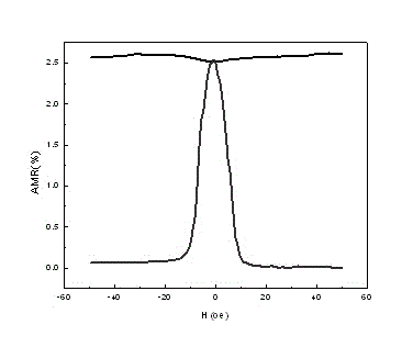
An anisotropic magnetic and permalloy technology, applied in metal material coating process, application of magnetic film to substrate, coating, etc., can solve the problem that the performance does not meet the requirements of use, the film AMR is small, and the coercive force It can reduce the coercivity, increase the AMR value, and increase the grain size.

Inactive Publication Date: 2015-03-25
GUIZHOU YAGUANG ELECTRONICS TECH
View PDF3 Cites 4 Cited by
  • Summary
  • Abstract
  • Description
  • Claims
  • Application Information

AI Technical Summary

Problems solved by technology

[0004] Although the above method is technically mature, for some products that require thin film patterning, it is necessary to use photoresist to photoetch the pattern on the silicon wafer, and then use it to deposit the thin film, which makes it impossible to use a heating substrate. However, the AMR of the film deposited at room temperature is very small, and the coercive force is very large. Even if it is annealed at high temperature afterwards, its performance cannot meet the requirements for use, which makes the use of this film very popular. very restrictive

Method used


Image

  • Anisotropic magnetoresistive permalloy buffer layer preparation method
  • Anisotropic magnetoresistive permalloy buffer layer preparation method
  • Anisotropic magnetoresistive permalloy buffer layer preparation method

Examples


Embodiment Construction

[0023] The present invention will be further described in detail below in conjunction with the accompanying drawings, but not as any limitation to the present invention.

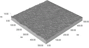
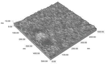
[0024] When implementing the preparation method of a kind of anisotropic magnetoresistive permalloy buffer layer of the present invention, as attached Figure 5 with 6 As shown, the method is implemented on the basis of the existing substrate, that is, the buffer layer is first deposited on the existing substrate, then the NiFe layer is deposited, and finally the protective layer is covered. The process of depositing the buffer layer is adopted in The pulsed radio frequency is used as the sputtering power source at normal temperature, and the structure prepared by the invention is consistent with the traditional structure.

[0025] The specific production process is to put the cleaned substrate (using silicon wafer) into the vacuum chamber and evacuate it to 5x10⁻⁵Pa, and pass in argon gas throughout the pro...


PUM

PropertyMeasurementUnit
surface roughnessaaaaaaaaaa

Abstract

The invention discloses an anisotropic magnetoresistive permalloy buffer layer preparation method. The method comprises the steps that a substrate which is thoroughly cleaned is put into a vacuum cavity, argon gas is provided in the whole process, a buffer layer is deposited by adopting the pulse radio frequency as a sputtering power source, then a NiFe layer is deposited, and finally a covering layer is deposited. The pulse radio frequency technology is adopted, power is supplied to a target gun at intervals during thin film deposition, time is provided for migration of material atoms on the surface of the substrate due to pulse radio frequency interval deposition, and the thin film flatness is improved, so that the crystalline degree of the thin film is enhanced, and the material AMR value is increased; by means of the pulse radio frequency deposition technology, the deposition atoms can sufficiently migrate on the surface of the substrate, the surface flatness of the buffer layer is improved, growth of the NiFe thin film structure can be better induced at normal temperature, and the crystalline grain diameter is increased, so that the permalloy thin film AMR value is increased, the coercive force is lowered, and the thin film sensitivity becomes better.

Description

technical field [0001] The invention relates to a method for preparing an anisotropic magnetic resistance permalloy buffer layer, belonging to the technical field of electronic product preparation. Background technique [0002] Permalloy thin film materials (mainly composed of Ni-Fe) with anisotropic magnetoresistance (AMR) effect are widely used in the production of various high-sensitivity magnetic sensors such as computer hard disk read heads, and are widely used in automation technology, household appliances, Navigation systems, mobile communications, mass storage and computers. At the same time, because the anisotropic magnetoresistivity is related to the angle of the magnetic field and the current, this material has a unique application prospect in the fields of geomagnetic navigation. The usual structure of this AMR thin film material is shown in the figure Figure 5 , first deposit a thinner buffer layer on the substrate, such as tantalum Ta, MgO or NiFeCr, then depo...

Claims


Application Information

Patent Timeline
Patent Type & Authority Applications(China)
IPC IPC(8): H01F41/14H01F41/18C23C14/34
Inventor 张文旭杨华彭斌余涛
Owner GUIZHOU YAGUANG ELECTRONICS TECH
Why Eureka
Try Eureka