Infrared detector array and manufacturing method thereof

A technology of infrared detectors and arrays, which is applied in semiconductor devices, final product manufacturing, radiation control devices, etc., can solve problems such as difficulty in realization and affecting the generation of photogenerated carriers, and achieve improved quantum efficiency, enhanced capabilities, and reduced The effect of crosstalk

Inactive Publication Date: 2015-03-25
XIDIAN UNIV
View PDF6 Cites 4 Cited by
  • Summary
  • Abstract
  • Description
  • Claims
  • Application Information

AI Technical Summary

Problems solved by technology

However, this invention requires the heteroepitaxial InSb material on the silicon substrate, which will cause a large number of dislocations or defects in the n-type InSb region, especially near the interface between the silicon substrate and the n-type InSb region, and affect the flow of photogenerated carriers. Generate and capture a large number of photogenerated carriers. In addition, the invention also needs to prepare silicon microlenses, so the invention is difficult to realize

Method used


Image

  • Infrared detector array and manufacturing method thereof
  • Infrared detector array and manufacturing method thereof
  • Infrared detector array and manufacturing method thereof

Examples


Embodiment 1

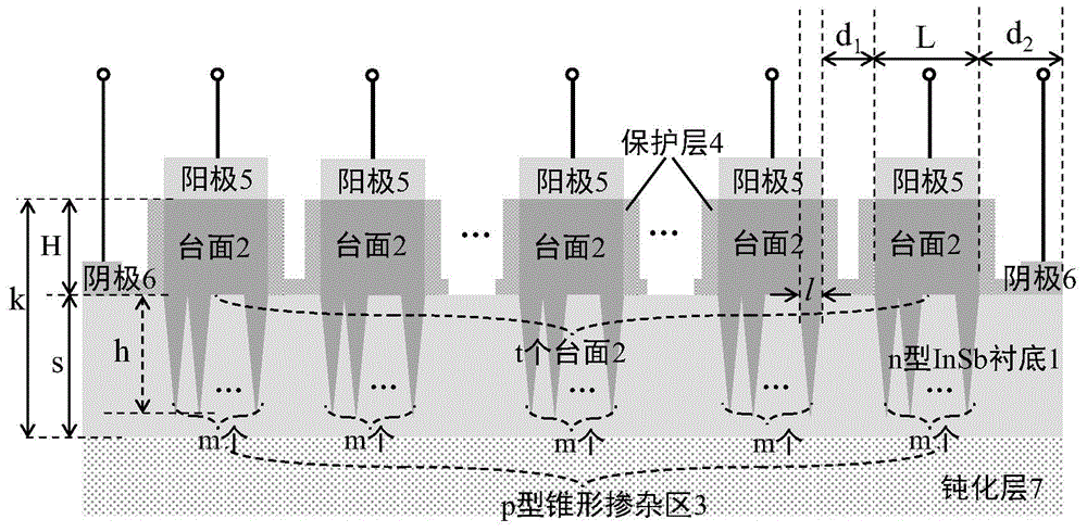
[0037] Embodiment 1: The protective layer is made of SiN, the passivation layer is made of SiN, the number of p-type conical doped regions directly below each mesa is m×m=4×4, and the array size is an infrared detector array of 30×30 .

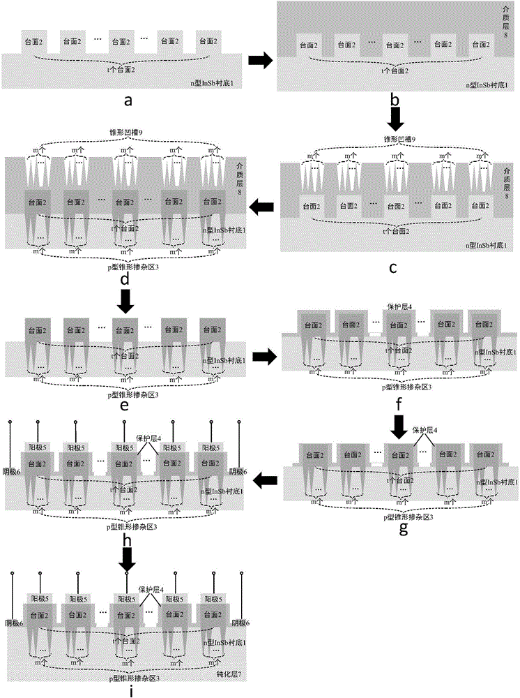
[0038] Step 1, etching and manufacturing 30×30 mesas 2 on the n-type InSb substrate 1, such as image 3 a.

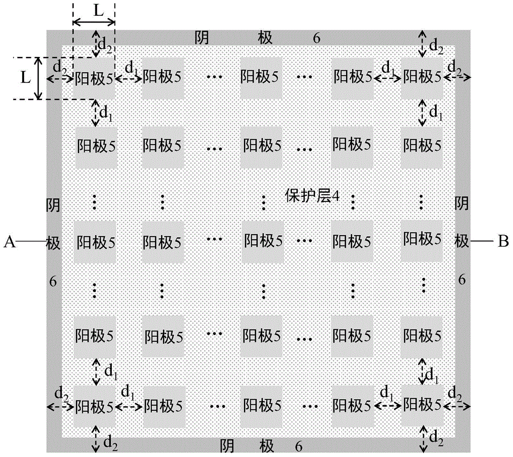
[0039] 1a) At a thickness k of 21 μm and a doping concentration of 1×10 16 cm -3 For the first time, a mask is made on the n-type InSb substrate 1. The mask pattern is an array composed of 30×30 squares with a side length L of 56 μm, and the distance between two adjacent squares is d 1 , and the distance d between the most edge square and the edge of n-type InSb substrate 1 2 Both are 45μm;

[0040] 1b) Use the mask to etch 30×30 mesas 2 on the n-type InSb substrate 1 by reactive ion etching technology, where the height H of each mesa is 12 μm. After the n-type InSb substrate 1 is etched The thickness s is 9 μm. The process condi...

Embodiment 2

[0066] Embodiment 2: Making the protective layer is SiO 2 , the passivation layer is SiO 2 , the number of p-type tapered doped regions directly below each mesa is m×m=2×2, and the array size is an infrared detector array of 512×512.

[0067] Step 1, etching and manufacturing 512×512 mesas 2 on the n-type InSb substrate 1, such as image 3 a.

[0068]At a thickness k of 11 μm and a doping concentration of 1×10 14 cm -3 The n-type InSb substrate 1 made a mask for the first time, using inductively coupled plasma reactive etching technology, in Ar / CH 4 / H 2 Under the process conditions of flow ratio of 1:3:10, pressure of 10Pa, and power of 550W, 512×512 square mesas with height H of 6 μm and side length L of 36 μm were etched on n-type InSb substrate 1 2, where the distance d between two adjacent mesa 1 , the distance d between the edge of the mesa and the edge of the n-type InSb substrate 1 2 Both are 20 μm; the thickness s of the n-type InSb substrate 1 after etching i...

Embodiment 3

[0085] Embodiment three: making protective layer is SiN, and passivation layer is SiO 2 , the number of p-type tapered doped regions directly below each mesa is m×m=1×1, and the array size is an infrared detector array of 10000×10000.

[0086] Step A, etching and manufacturing 10000×10000 mesas 2 on the n-type InSb substrate 1, such as image 3 a.

[0087] At a thickness k of 2.6 μm and a doping concentration of 1×10 11 cm -3 Masks were fabricated on the n-type InSb substrate 1 for the first time, and 10,000×10,000 square mesas 2 with a side length of 8 μm were etched on the n-type InSb substrate 1 by inductively coupled plasma reactive etching technology. The distance d between two tables 1 , the distance d between the edge of the mesa 2 and the edge of the n-type InSb substrate 1 2 Both are 0.5 μm, and the height H of each mesa is 0.6 μm; the thickness s of the n-type InSb substrate 1 after etching is 2 μm. The process conditions used for etching the mesa are: Ar / CH 4...


PUM


Abstract

The invention discloses an infrared detector array and a manufacturing method of the infrared detector array. The detector array comprises an n-type InSb substrate (1) and a passivation layer (7), t*t tabletops (2) are etched on the n-type InSb substrate (1), wherein t is an integer and is greater than or equal to one; an anode (5) is deposited on each tabletop (2), and an cathode (6) shaped like the Chinese character 'hui' is deposited on the upper portion of the edge of the n-type InSb substrate (1); the upper portion of the n-type InSb substrate (1) and the side face of each tabletop (2) are each provided with a protection layer (4) in a deposited mode; m*m identical p-type conical doping areas (3) are arranged in the positions, under each tabletop (2), of the n-type InSb substrate (1) to from a p-type conical doping area array, and one pn junction is formed between each p-type conical doping area (3) and the n-type InSb substrate (1), wherein m is an integer and is greater than or equal to one. The infrared detector array has the advantages of being simple in process, high in quantum efficiency and low in crosstalk, and can be used for the fields of infrared investigation and infrared medical treatment.

Description

technical field [0001] The invention belongs to the technical field of semiconductor photovoltaic detection devices, in particular to an infrared detector array, which can be used for infrared detection, infrared guidance and infrared medical treatment. technical background [0002] The core component of the infrared focal plane array infrared system, its function is to convert infrared radiation into other signals that we can recognize. It has important and extensive applications in military and civilian fields such as space ground observation, photoelectric countermeasures, robot vision, medical and industrial thermal imaging, search and tracking, and missile precision guidance. High-performance large-scale infrared focal plane arrays have been widely used It is used in various major national security projects and important new weapon systems. Because of its irreplaceable status and role, major industrial countries in the world have listed the preparation technology of in...

Claims


Application Information

Patent Timeline
Patent Type & Authority Applications(China)
IPC IPC(8): H01L27/146H01L31/18
CPCY02P70/50
Inventor 杨翠张延涛马京立陈园园陈晓冬孟超张小雷毛维吕衍秋司俊杰
Owner XIDIAN UNIV
Why Eureka
Try Eureka