(111) Three-axis micromachined acceleration sensor integrated on a single silicon chip and its manufacturing method

An acceleration sensor and acceleration sensing technology, which are used in multi-dimensional acceleration measurement, acceleration measurement using inertial force, and microstructure devices composed of deformable elements, which can solve the problems of complex manufacturing process, difficult to meet detection, large size, etc. problems, to achieve good process compatibility, reduce production costs, and simplify the production process.

Active Publication Date: 2017-10-27
SHANGHAI INST OF MICROSYSTEM & INFORMATION TECH CHINESE ACAD OF SCI
View PDF5 Cites 0 Cited by
  • Summary
  • Abstract
  • Description
  • Claims
  • Application Information

AI Technical Summary

Problems solved by technology

[0005] In view of the above-mentioned shortcoming of prior art, the object of the present invention is to provide a kind of (111) three-axis micro-machine acceleration sensor integrated with single silicon chip and manufacturing method, be used to solve the three-axis micro-machine acceleration sensor in the prior art Difficult to meet ultra-high g range (>70,000 g) detection, and the existing problems of high cost, large size, low strength and complex manufacturing process

Method used


Image

  • (111) Three-axis micromachined acceleration sensor integrated on a single silicon chip and its manufacturing method
  • (111) Three-axis micromachined acceleration sensor integrated on a single silicon chip and its manufacturing method
  • (111) Three-axis micromachined acceleration sensor integrated on a single silicon chip and its manufacturing method

Examples


Embodiment 1

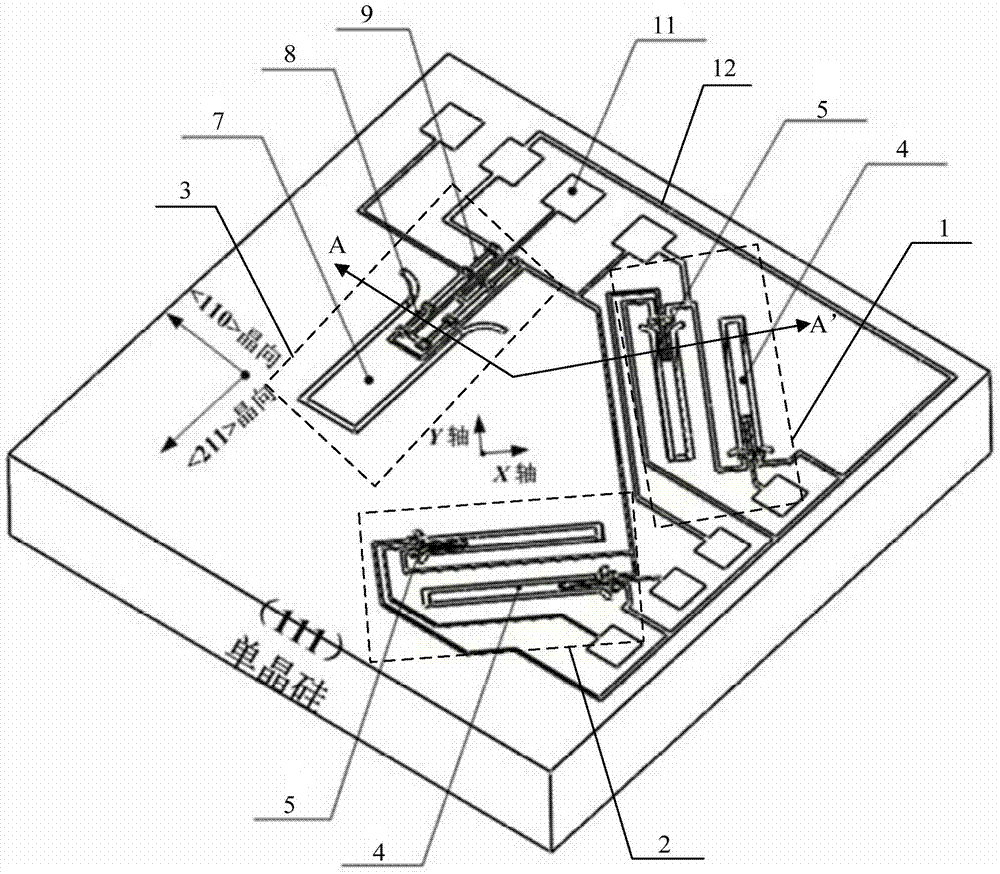
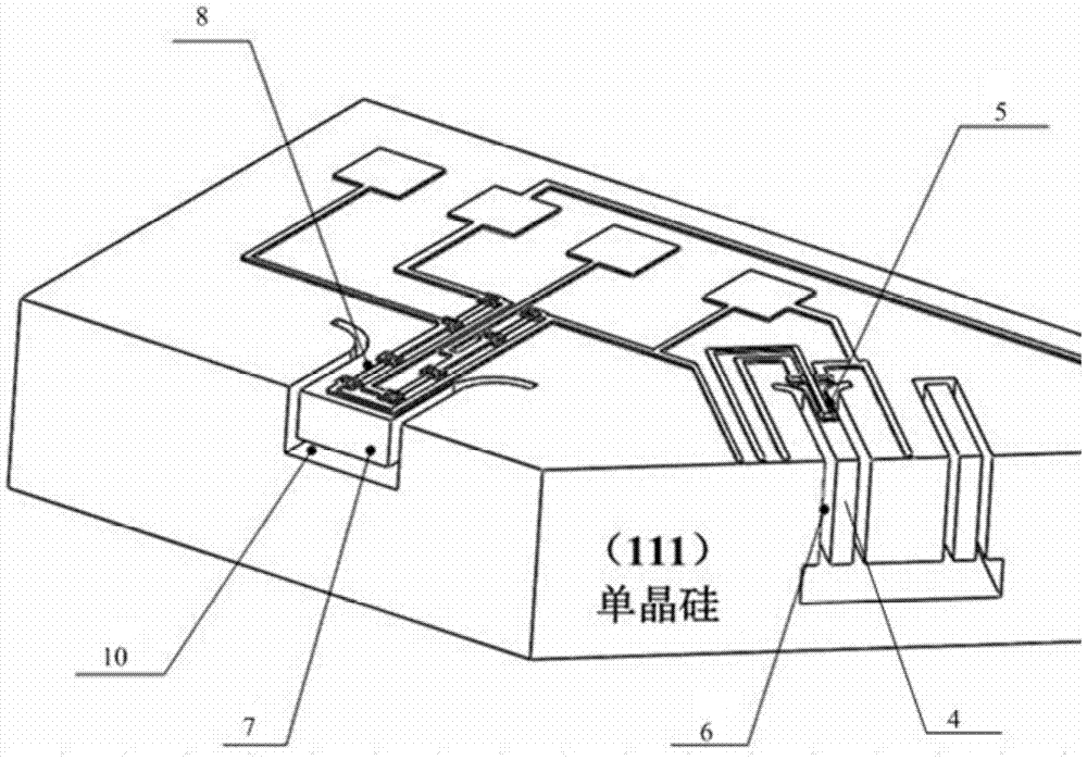
[0047] see figure 1 , the present invention provides a (111) three-axis micromachined acceleration sensor integrated with a single silicon chip, the (111) three-axis micromachined acceleration sensor integrated with a single silicon chip at least includes: (111) a single silicon chip and all integrated in Three mutually independent acceleration sensing units 1 in the X-axis direction, 2 acceleration sensing units 2 in the Y-axis direction and 3 acceleration sensing units 3 in the Z-axis direction on the (111) single silicon chip; The acceleration sensing unit 1, the acceleration sensing unit 2 in the Y-axis direction, and the acceleration sensing unit 3 in the Z-axis direction are integrated on the same surface of the (111) single silicon chip; wherein, the acceleration in the X-axis direction The sensing unit 1 has the same structure as the acceleration sensing unit 2 in the Y-axis direction, and both include a first cantilever beam 4 and a first pressure-sensitive resistor 5...

Embodiment 2

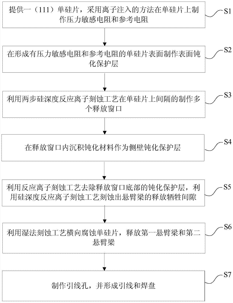
[0060] see Figure 3 to Figure 4 , the present invention also provides a (111) manufacturing method of a three-axis micromachined acceleration sensor integrated on a single silicon chip, comprising the following steps:

[0061] 1) An n-type (111) single silicon wafer is provided, the single-sided polished or double-sided polished silicon wafer, and the axis offcut is 0±0.1°; the method of boron ion implantation is used on the (111) single silicon wafer Make pressure-sensitive resistors and reference resistors on the front side, and the resistance value of the resistors is 2.0kΩ~3.0kΩ (such as Figure 4 (a) shown).

[0062] 2) Depositing low-stress silicon nitride and TEOS silicon oxide sequentially on the front side of the (111) single silicon wafer as a surface passivation protection layer by using LPCVD process.

[0063] 3) Using a two-step silicon deep reactive ion etching process to make a plurality of release windows at intervals on the (111) single silicon wafer, the r...


PUM

PropertyMeasurementUnit
angleaaaaaaaaaa
lengthaaaaaaaaaa
thicknessaaaaaaaaaa

Abstract

The invention provides a (111) single-silicon-chip integrated three-axis micro-mechanical acceleration sensor and a manufacturing method. The three-axis acceleration sensor adopts a single-silicon monohedral silicon micro-mechanical process, and is manufactured by one-time molding on the same surface of a (111) single-silicon wafer. Among them, the acceleration sensing unit in the X-axis and Y-axis directions adopts a double cantilever beam structure, and the acceleration sensing unit in the Z-axis direction adopts a single cantilever beam structure. The sensitive structures of cantilever beams of different sizes are realized by selective etching inside the single silicon substrate. One release molding. The pressure film damping and overload protection in the sensitive direction of the acceleration sensing unit in the Z-axis direction are adjusted by the movable gap buried inside the single crystal silicon substrate, which solves the residual stress caused by the multi-chip bonding of traditional multi-axis sensors , poor impact strength and high production costs. It has the advantages of small size, low cost, strong process compatibility, suitable for high-g acceleration measurement, etc., and has broad application prospects.

Description

technical field [0001] The invention belongs to the field of silicon micromechanical sensors, and relates to a (111) three-axis micromechanical acceleration sensor integrated with a single silicon chip and a manufacturing method. Background technique [0002] With the rapid development of MEMS technology and the maturity of silicon micromachining technology, accelerometers based on silicon micromachining technology have the advantages of small size, low cost, high performance and suitable for mass production. It is widely used in different fields and plays an important role, such as: automotive airbags, crash testing, consumer electronics, seismic wave detection, military inertial technology navigation, robot industry and automation control and other motion monitoring projects. Among them, explosion, impact and penetrating bomb fuzes are one of the very special applications, and the acceleration that needs to be detected can reach the level of tens of thousands of g or even ...

Claims


Application Information

Patent Timeline
Patent Type & Authority Patents(China)
IPC IPC(8): G01P15/18B81B3/00B81C1/00
Inventor 李昕欣王家畴邹宏硕
Owner SHANGHAI INST OF MICROSYSTEM & INFORMATION TECH CHINESE ACAD OF SCI
Why Eureka
Try Eureka