Process for processing surface plasmon polariton coupled nano array based on scallop effect

A surface plasmon and nanoarray technology, applied in the field of plasmonic coupled nanoarrays, can solve the problems of poor controllability and limited practicality, and achieve the effect of optimizing the design of the coupling structure and facilitating process integration

Active Publication Date: 2015-04-08
PEKING UNIV
View PDF7 Cites 27 Cited by
  • Summary
  • Abstract
  • Description
  • Claims
  • Application Information

AI Technical Summary

Problems solved by technology

At present, the research on the LSP-SPP coupling effect mostly adopts the self-assembly method of the coupling agent to construct the "noble metal nanoparticle-polymer-metal

Method used


Image

  • Process for processing surface plasmon polariton coupled nano array based on scallop effect
  • Process for processing surface plasmon polariton coupled nano array based on scallop effect
  • Process for processing surface plasmon polariton coupled nano array based on scallop effect

Examples


Embodiment Construction

[0022] The present invention will be described in detail below in conjunction with the accompanying drawings and examples.

[0023] The present invention utilizes deep reactive ion etching of traditional microelectronics technology (formation of scallop topography sidewall by alternating etching and passivation——Scallop effect) and electron beam exposure (for making photolithography mask with nanoscale precision) technology , proposed a three-dimensional nano-optical structure processing technology combining electron beam exposure and deep reactive ion etching, and prepared functional units of "metallized nanostructure-spacer layer-metal film" and their periodic arrangement of "LSP-SPP coupling "Nanoarrays.

[0024] The principle of the "LSP-SPP coupling" nano-array processing technology of the present invention is as follows:

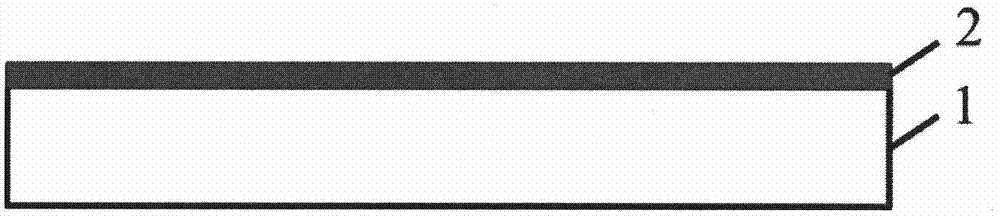
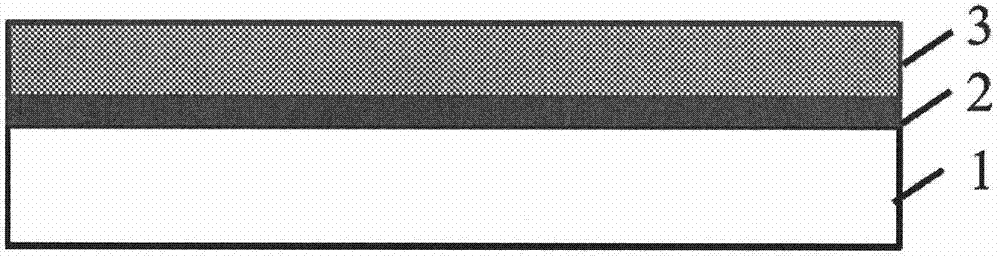
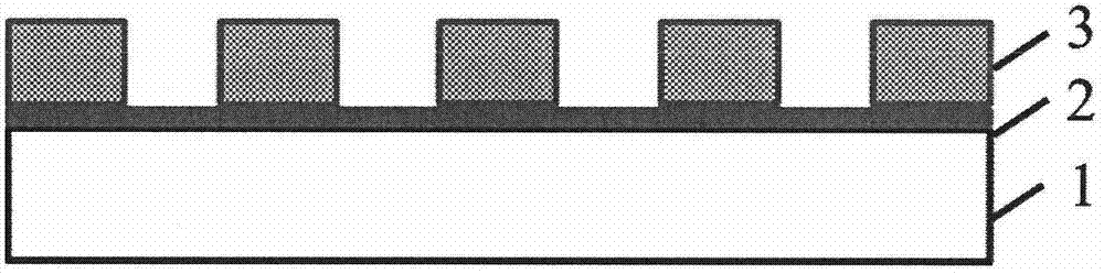
[0025] Such as Figure 1-7 As shown, an etch mask layer 2 is deposited on a substrate 1 (such as a silicon wafer) such as figure 1 , spin-coated e-...


PUM


Abstract

The invention discloses a method for preparing a surface plasmon polariton coupled nano array. The method comprises the following steps: performing deep reactive ion etching on a substrate by adopting a nano-scale etching mask which is manufactured by electron beam exposure, and then performing metallic membrane plating to obtain a three-dimensional 'metal nano structure array-nano space layer-metallic film' structure. The metallic nano structure generates local electromagnetic field resonance of photon and free electron to generate a very strong local surface plasmon polariton, and a diffraction effect provides wave vector compensation to excite a propagating type surface plasmon polariton of the metallic film so as to form local surface plasmon polariton-propagating type surface plasmon polariton coupling, so that light is restrained in a nano scale to initiate very strong surface local near field enhancement between a metal and a medium interface. The structure manufactured by the process disclosed by the invention can promote new mechanism exploration of the surface plasmon polariton, and has important application prospects in the fields of metamaterials, ultrahigh-sensitivity optical biosensing and the like.

Description

technical field [0001] The invention relates to a periodic surface plasmon coupling nano-array structure processing technology, in particular to preparing a surface plasmon coupling nano-array by combining electron beam lithography and reactive ion deep etching technology. This method uses the characteristics of electron beam direct writing nanoscale precision template and the "scallop effect" of reactive ion etching side wall surface to process "metallized nanostructures" with the optical coupling effect of localized surface plasmons and surface propagating plasmons. Structure-spacer layer-metal film" functional unit and its periodically arranged nano-arrays. Background technique [0002] The "metallized nanostructure-spacer layer-metal thin film" surface plasmon coupled nanostructure not only has a tip effect, that is, a strong local electromagnetic field is generated at the tip to form a non-propagating surface-bound mode - localized surface plasmon resonance (LSPR), and...

Claims


Application Information

Patent Timeline
IPC IPC(8): B81C1/00
Inventor 吴文刚樊姣荣马鹏程谌灼杰
Owner PEKING UNIV
Why Eureka
Try Eureka