Producing method for graphical sapphire substrate

A technology of sapphire substrate and manufacturing method, which is applied in the direction of electrical components, circuits, semiconductor devices, etc., can solve problems such as increased leakage current, increased epitaxial growth cycle, lattice mismatch, etc., to increase lateral epitaxial growth, reduce Epitaxial growth cycle, the effect of increasing the probability of exit

Inactive Publication Date: 2015-04-29
SHENZHEN DESUN PHOTOELECTRICITY
View PDF3 Cites 7 Cited by
  • Summary
  • Abstract
  • Description
  • Claims
  • Application Information

AI Technical Summary

Problems solved by technology

[0003] At present, most LED epitaxial layers are prepared by metal-organic chemical vapor deposition (MOCVD) heterogeneous epitaxy. Due to the inconsistent lattice mismatch and thermal mismatch between the substrate and the epitaxy, this will lead to poor quality of the grown epitaxial crystal. In order to improve the crystal quality, researchers use buffer layer technology to improve the epitaxial crystal quality, and the effect is remarkable, but there is still a high dislocation density in the epitaxial layer
High dislocation density leads to increased leakage current, reduced efficiency and reduced lifetime of the device. In order to further improve the crystal quality of the epitaxial layer, the researchers adopted the lateral epitaxy technique (ELOG), which uses the blocking and steering of dislocations to make threading dislocations Termination, cannot continue to expand upward to the light-emitting region, improve the quality of epitaxial crystals, and improve device performance. At present, the most used surface patterned substrate technology (PSS), which not only enables epitaxy to use lateral epitaxy during the growth process to reduce dislocations Density, improve crystal quality, and can also use PSS pattern to reflect the light from the light-emitting area to the substrate through different surfaces, improve the probability of light escape, and improve the light output efficiency of the chip
[0004] Although lateral epitaxy can improve crystal quality, there are still some problems, such as figure 1 As shown in (a), for lateral epitaxy, because the threading dislocation in vertical epitaxy is consistent with the crystal growth direction, the dislocation line will extend to the light-emitting region along the crystal growth direction, affecting the performance of the device, while the lateral epitaxy The dislocations will be terminated at the interface, so to use lateral epitaxy to reduce defect density, it is necessary to avoid epitaxial growth in the vertical direction and increase epitaxial growth in the side direction, so as to improve the quality of epitaxial crystals, reduce defect density, and improve chip luminescence strength and reliability
[0005] In addition to the above, the gap of the patterned substrate has a certain depth. If the depth is too low, the probability of light escape will not be greatly improved. If the depth is too high, it will cost more during the epitaxy growth process. time to fill these gaps, which will increase the epitaxial growth cycle

Method used


Image

  • Producing method for graphical sapphire substrate
  • Producing method for graphical sapphire substrate

Examples


Embodiment 1

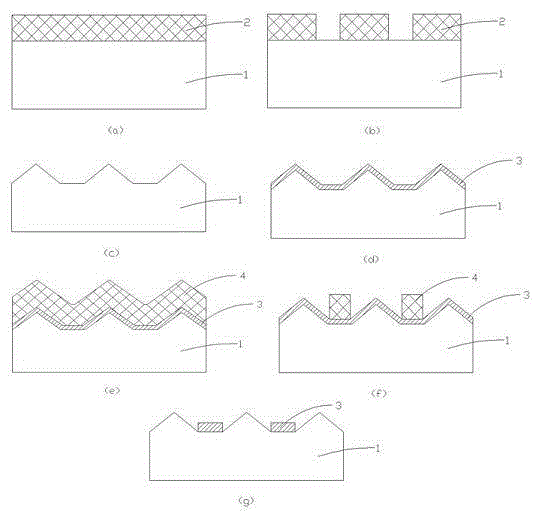
[0048] This embodiment combines figure 1 As shown, this embodiment adopts a patterned substrate obtained by a dry method.

[0049] 1. Provide a flat sapphire substrate 1 with a first layer of photoresist 2 of 2.5 μm on its surface, such as figure 1 as shown in (a);

[0050] 2. Use photolithography technology to expose the first layer of photoresist 2, and form such as figure 1 the graph shown in (b);

[0051] 3. Using the ICP process, using boron trichloride gas to etch a pattern on the surface of the substrate 1, remove the remaining first layer of photoresist 2, and form such as figure 1 (c) the graph shown;

[0052] 4. Deposit 200nm silicon dioxide 3 on the surface of the patterned substrate 1 by plasma enhanced chemical vapor deposition, such as figure 1 as shown in (d);

[0053] 5. Utilize photolithography technology to expose the second layer of photoresist 4, and form such as figure 1 (f) the graph shown;

[0054] 6. Corrosion of silicon dioxide 3 formation fig...

Embodiment 2

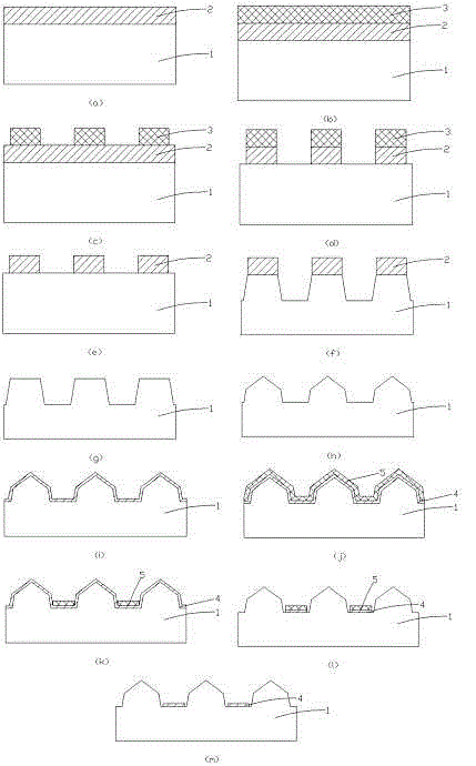
[0056] This embodiment combines figure 2 As shown, this embodiment uses a patterned substrate obtained by a wet method.

[0057] 1. A flat sapphire substrate 1 is provided, and a first layer of silicon dioxide 2 of 100 nm is deposited on its surface by plasma-enhanced chemical vapor deposition, such as figure 2 as shown in (a);

[0058] 2. Use photolithography to expose the photoresist to form such as figure 2 The graph shown in (c), the detailed process see figure 2 (b) and 2(c);

[0059] 3. Etch the first layer of silicon dioxide 2 to obtain such figure 2 The graph shown in (e), the specific process is detailed in figure 2 (d) and 2(e);

[0060] 4. Use 270°C, soak in the mixed acid solution of phosphoric acid: sulfuric acid = 1:3 for a certain period of time, and obtain the following figure 2 The pattern shown in (g), then remove the first layer of silicon dioxide 2 on the surface, and keep the first layer of photoresist 3, the specific process is detailed in f...


PUM

PropertyMeasurementUnit
thicknessaaaaaaaaaa
thicknessaaaaaaaaaa

Abstract

The invention discloses a producing method for a graphical sapphire substrate. A flat substrate is provided; a mask layer is formed on the surface; a graphical mask layer is produced on the surface of the mask layer by utilizing a photolithography; a graph is formed on the surface of the substrate by adopting a wet process corrosion or dry process etching technology by utilizing the graphical mask layer; the mask layer is removed; an insulating medium film is formed on the surface of the graphical substrate; the insulating medium film in the clearance of the graphical substrate is protected by utilizing the photolithography; the insulating medium film out of the photolithography protection is removed by adopting the wet process corrosion or dry process etching technology. According to the invention, epitaxy cannot grow on the surface of the insulating medium film; the epitaxial growth in the vertical direction is avoided; lateral epitaxial growth is increased; the dislocation density in a glowing area is reduced; the insulating medium film with certain film thickness is adopted to fill the clearance of the graphical substrate; the depth of the clearance is reduced; epitaxial growth cycle is reduced.

Description

technical field [0001] The invention relates to the field of semiconductor optoelectronic chip manufacturing, in particular to a substrate patterning technology for improving the effect of lateral epitaxy. Background technique [0002] Semiconductor light-emitting diode (LED) is a new type of solid-state cold light source. Its high energy efficiency, long life, small size, low voltage and many other advantages make it widely used in people's daily life, traffic lights, headlights, outdoor displays, mobile phone backlights Sources, electrical indicator lights, and some lighting street lights are widely used in large numbers. Especially in terms of energy saving and environmental protection, LED lamps have obvious advantages over ordinary incandescent lamps and fluorescent lamps, so it has become a consensus to replace traditional light sources as the main lighting source in the future. [0003] At present, most LED epitaxial layers are prepared by metal-organic chemical vapo...

Claims


Application Information

Patent Timeline
Patent Type & Authority Applications(China)
IPC IPC(8): H01L33/00
CPCH01L33/005H01L2933/0008
Inventor 夏鼎智
Owner SHENZHEN DESUN PHOTOELECTRICITY
Why Eureka
Try Eureka