Supercharge Your Innovation With Domain-Expert AI Agents!

Printed fixed-point growth method of two-dimensional chalcogenide crystals

A chalcogen and crystal technology, applied in crystal growth, single crystal growth, single crystal growth, etc., can solve difficult problems

Active Publication Date: 2017-11-21
PEKING UNIV
View PDF1 Cites 1 Cited by
  • Summary
  • Abstract
  • Description
  • Claims
  • Application Information

AI Technical Summary

Problems solved by technology

These methods have their own advantages, but it is difficult to control the nucleation position, shape, orientation and thickness of high-quality two-dimensional chalcogen atom crystals at the same time. In order to build an integrated device, it is necessary to simultaneously realize these parameters. regulation to achieve fixed-point growth

Method used


Image

  • Printed fixed-point growth method of two-dimensional chalcogenide crystals
  • Printed fixed-point growth method of two-dimensional chalcogenide crystals
  • Printed fixed-point growth method of two-dimensional chalcogenide crystals

Examples


Embodiment 1

[0071] Example 1. Controllable preparation of two-dimensional chalcogen atom crystal arrays

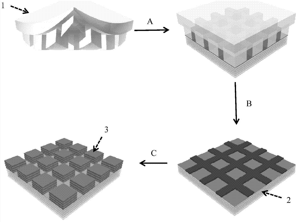
[0072] 1) will be as image 3 The array-type PDMS elastic stamp shown is soaked in ethanol liquid, and the PDMS oligomer is dissolved to form ink, which is then directly imprinted on the surface of the freshly peeled fluorophlogopite substrate with a thickness of 2 mm. The ethanol is completely volatilized by heating or vacuum drying to obtain a patterned and modified fluorophlogopite substrate.

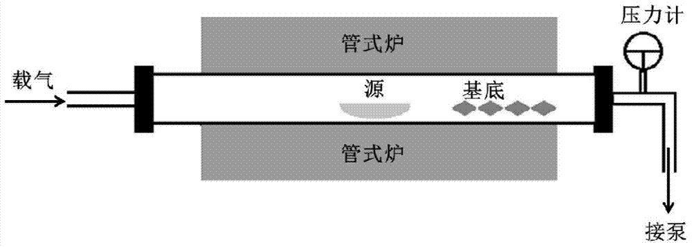
[0073] 2) The source (chalcogenide material In 2 Se 3 、 Bi 2 Se 3 , SnSe or GaSe) are ground into powder and placed in a semicircular quartz boat, placed in the center of the quartz tube, and the resulting patterned modified fluorophlogopite substrate is placed on the quartz at a distance of 7 to 16 cm from the source downstream of the airflow direction. In the tube, the deposition temperature of the patterned and modified fluorophlogopite substrate obtained in step 1) is 50-250°C lower...

Embodiment 2

[0096] Example 2, the shape controllable preparation of two-dimensional chalcogen atom crystals

[0097] The specific operation steps of this embodiment are the same as those of Embodiment 1, except that PDMS elastic stamps with different shapes are used for growth to obtain a two-dimensional chalcogen atom crystal with the same shape as the stamp. This shows that the present invention can prepare shape-controllable two-dimensional chalcogen atom crystals. In this embodiment, the high-purity argon flow rate is 200 standard cubic centimeters per minute, and the system pressure is 6.7 kPa. In the physical vapor deposition, the growth was carried out at 490 degrees Celsius for 10 minutes.

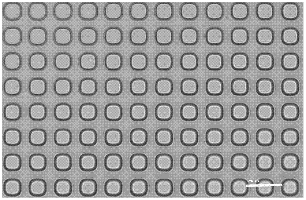
[0098] Figure 21 is an optical microscope image of a continuous grid-like PDMS elastic stamp.

[0099] Figure 22 is to use Figure 21 The grid-like continuous Bi obtained from the stamp growth shown 2 Se 3 Optical microscope image of a 2D atomic crystal.

[0100] Figure 23 is to us...


PUM

PropertyMeasurementUnit
thicknessaaaaaaaaaa
thicknessaaaaaaaaaa

Abstract

The invention discloses a method for printing type fixed point growth of two-dimensional sulfur group crystals. The method comprises the following steps: (1) soaking an elastic stamp in a volatile solvent, taking out the elastic stamp, stamping the elastic stamp on the surface of a substrate, and peeling off the substrate from the elastic stamp when the volatile solvent is volatilized to obtain a patterning modified substrate; and (2) sequentially placing the patterning modified substrate and a sulfur group material to perform physical vapor deposition in a non-oxidizing atmosphere according to a sequence from downstream to upstream of a gas path, and cooling after deposition to obtain the two-dimensional sulfur group crystals. The invention develops a universal method for controlling the growth of two-dimensional sulfur group atomic crystals; and by adopting the method, the two-dimensional sulfur group atomic crystals with large areas, high-quality shapes and controllable nucleation sites, orientation and thicknesses can be obtained. A two-dimensional sulfur group atomic crystal array prepared by the method can be transferred to any other substrate, and has an important potential application in the fields of photoelectric detection and the like.

Description

technical field [0001] The invention relates to a printing type fixed-point growth method of two-dimensional chalcogenide crystals. Background technique [0002] Two-dimensional atomic crystal refers to a new type of two-dimensional crystal material with a single or a few atomic layer thickness mainly formed by covalent bonding. Two-dimensional chalcogen atom crystals are one of the families with a wide variety and rich properties, all of which contain one or more of the chalcogen elements sulfur, selenium, and tellurium in composition. Structurally, two-dimensional chalcogen atom crystals are composed of multiple layer structural units formed by alternating atomic layers. The multilayers are connected by strong covalent bonds, and the interlayers are connected by weak van der Waals forces, forming a highly anisotropic structure. There are more than sixty types of two-dimensional chalcogenide atomic crystals, and their bulk material properties are very rich, covering metal...

Claims


Application Information

Patent Timeline
Patent Type & Authority Patents(China)
IPC IPC(8): C23C14/04C23C14/06C30B23/00C30B29/46
CPCC23C14/04C23C14/06C30B23/00C30B29/46
Inventor 彭海琳郑文山谢天周喻刘忠范
Owner PEKING UNIV
Features
  • R&D
  • Intellectual Property
  • Life Sciences
  • Materials
  • Tech Scout
  • Unparalleled Data Quality
  • Higher Quality Content
  • 60% Fewer Hallucinations
Learn More