TFT backboard manufacturing method and structure suitable for AMOLED

A manufacturing method and backplane technology, applied in semiconductor/solid-state device manufacturing, semiconductor devices, electrical components, etc., can solve problems such as low manufacturing efficiency and cumbersome manufacturing process, and achieve increased manufacturing process, simple manufacturing process, and reduced number of manufacturing processes Effect

Inactive Publication Date: 2015-05-27
TCL CHINA STAR OPTOELECTRONICS TECH CO LTD +1
View PDF3 Cites 33 Cited by
  • Summary
  • Abstract
  • Description
  • Claims
  • Application Information

AI Technical Summary

Problems solved by technology

In this manufacturing method, it is necessary to deposit two layers of gate insulating layers to increase the subthreshold swing of the driving thin film transistor T2, the manufacturing process is cumbersome, and the manufacturing efficiency is low.

Method used


Image

  • TFT backboard manufacturing method and structure suitable for AMOLED
  • TFT backboard manufacturing method and structure suitable for AMOLED
  • TFT backboard manufacturing method and structure suitable for AMOLED

Examples


Embodiment Construction

[0048] In order to further illustrate the technical means adopted by the present invention and its effects, the following describes in detail in conjunction with preferred embodiments of the present invention and accompanying drawings.

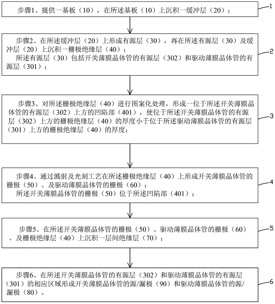
[0049] see figure 2 , the present invention firstly provides a method for manufacturing a TFT backplane suitable for AMOLED, comprising the following steps:

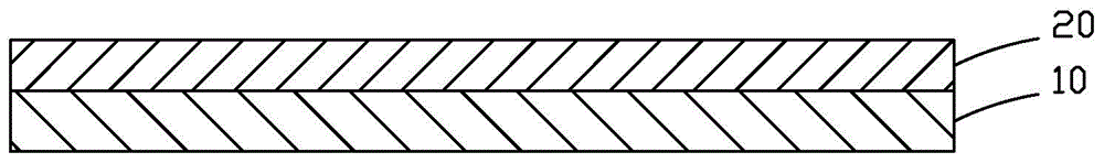
[0050] Step 1, such as image 3 As shown, a substrate 10 is provided, and a buffer layer 20 is deposited on the substrate 10 .

[0051] Specifically, the substrate 10 is a transparent substrate, preferably, the substrate 10 is a glass substrate. The buffer layer 20 includes one of a silicon oxide layer, a silicon nitride layer or a combination thereof.

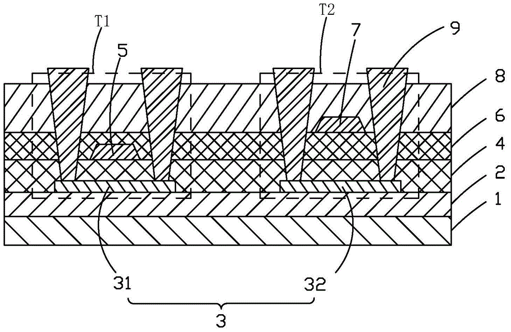
[0052] Step 2, such as Figure 4 As shown, an active layer 30 is formed on the buffer layer 20 , and a gate insulating layer 40 is deposited on the active layer 30 and the buffer layer 20 .

[0053] The active layer 30 includes an ...


PUM


Abstract

The invention provides a TFT backboard manufacturing method and structure suitable for AMOLED. The method comprises the following steps: 1, providing a baseboard (10) and depositing a buffer layer (20); 2, forming a source layer (30) and a gate insulation layer (40) on the buffer layer (20) in sequence; 3, carrying out patterning processing on the gate insulation layer (40) to form a recession part (401); 4, forming a gate (50) for switching a thin film transistor and a gate (60) for driving the thin film transistor, wherein the gate (50) for switching the thin film transistor is positioned at the recession part (401); 5, depositing an interlayer insulation layer (70). According to the method, a single-layer gate insulation layer with height different is manufactured, so that the manufacturing process of the TFT backboards is simplified, the subthreshold swing of the gate (60) for driving the thin film transistor and the grey scale switching and control properties of the AMOLED panes are improved.

Description

technical field [0001] The invention relates to the field of display technology, in particular to a manufacturing method and structure of a TFT backplane suitable for AMOLED. Background technique [0002] Flat-panel display devices have many advantages such as thin body, power saving, and no radiation, and have been widely used. Existing flat panel display devices mainly include liquid crystal display devices (Liquid Crystal Display, LCD) and organic light emitting diode display devices (Organic Light Emitting Display, OLED). [0003] Organic light-emitting diode display devices have excellent characteristics such as self-illumination, no need for backlight, high contrast, thin thickness, wide viewing angle, fast response speed, flexible panels, wide operating temperature range, and simple structure and manufacturing process. It is considered as an emerging application technology for the next generation of flat panel displays. [0004] OLEDs can be classified into passive ...

Claims


Application Information

Patent Timeline
Patent Type & Authority Applications(China)
IPC IPC(8): H01L51/56H01L51/52
CPCH01L27/1237H01L27/1248H01L27/1274H10K59/1213H10K50/00H10K59/1201H01L21/02164H01L21/0217H01L21/02271H01L21/02532H01L21/02592H01L21/02675H01L21/26506H01L21/28079H01L21/2855H01L21/28568H01L27/1218H01L27/1222H01L29/66757H01L29/78675
Inventor 张占东
Owner TCL CHINA STAR OPTOELECTRONICS TECH CO LTD
Why Eureka
Try Eureka