Hole metallization method based on laser activation technology

A technology of hole metallization and laser activation, which is applied to the formation of electrical connections of printed components, electrical components, and printed circuit manufacturing. It can solve the problems of affecting the quality of the coating, the degree of treatment is difficult to control, and the service life is reduced, so as to achieve good adhesion of the coating. Effect

Active Publication Date: 2015-05-27
ZHUHAI YUANSHENG ELECTRONICS SCI & TECH
View PDF5 Cites 4 Cited by
  • Summary
  • Abstract
  • Description
  • Claims
  • Application Information

AI Technical Summary

Problems solved by technology

However, this method has many limitations. Different formulas need to be adjusted when the materials used are different, and the degree of treatment is not easy to control, which can easily reduce the surface smoothness of the material and affect the quality of subsequent coatings; etching and roughening the material can easily lead to Aging, shortened lifespan; In addition, the introduction of chemicals has also brought environmental health and other issues

Method used


Image

  • Hole metallization method based on laser activation technology
  • Hole metallization method based on laser activation technology
  • Hole metallization method based on laser activation technology

Examples


Embodiment 1

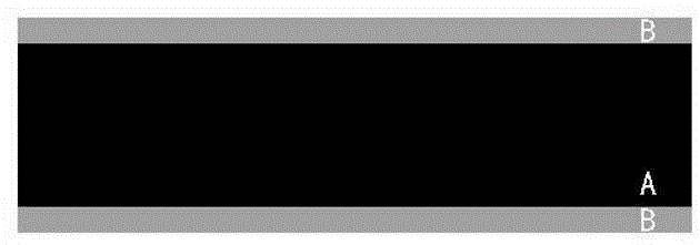
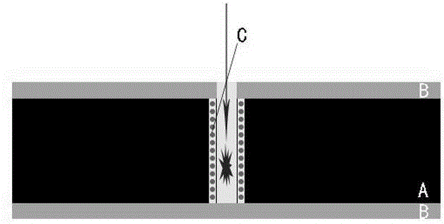
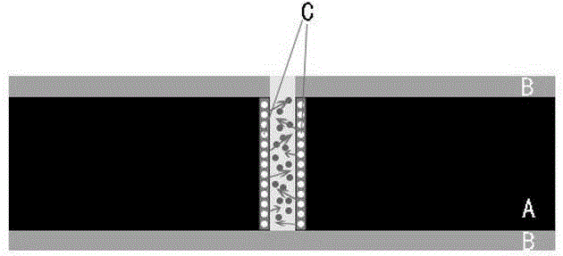
[0036] The double-sided copper-clad soft board is used as the base material, and blind hole metallization is realized to achieve the purpose of electrical connection.

[0037] (1) Select the polyimide double-sided copper-clad laminate commonly used in the market, which is mechanically processed and has excellent flexibility, as the base material, and cut it into a size suitable for processing.

[0038] (2) Put the material in the laser processing equipment. After the equipment enters the laser operation file, laser drilling is performed on the copper clad laminate (hereinafter referred to as the drilled hole is a micro hole, the same as in the second embodiment), and the laser irradiation is adjusted at the same time to make the surface form nanoscale pores. The laser irradiation pulse energy is controlled at 60-70 mJ, the focus height is controlled at 1.8 mm, the laser frequency is controlled at 50-60 kHz, the laser pulse width is controlled at 102-120 nms, and the beam diame...

Embodiment 2

[0047] The impregnated well-known glass fiber is used as the base material, and the metallization of the blind hole is realized to achieve the purpose of electrical connection.

[0048] (1) Select FR4, which is commonly used in the market and has excellent mechanical properties, as the base material, and cut it into a size suitable for processing.

[0049] (2) Put the material in the laser processing equipment. After the equipment enters the laser operation file, laser drilling is performed on the copper clad laminate, and the laser irradiation is adjusted at the same time to form nano-scale holes on the surface. The pulse energy of the laser irradiation meter is controlled at 100-125 mJ, the focus height is controlled at 10-30 mm, the laser frequency is controlled at 48-60 kHz, the laser pulse width is controlled at 102-120 nm, and the beam diameter is controlled at 15-20 mm.

[0050] (3) Put the drilled substrate into the plasma cleaning equipment to clean the tiny holes on ...


PUM

PropertyMeasurementUnit
thicknessaaaaaaaaaa
particle diameteraaaaaaaaaa

Abstract

The invention discloses a hole metallization method based on a laser activation technology. The method comprises steps as follows: holes are drilled in a printed circuit board base material with lasers, and special laser radiation is adjusted, so that drilled hole walls form nanoscale holes; catalytic particles permeate the holes to adsorb the hole walls to form an activation catalyst layer; finally, metal is deposited on hole wall surfaces by the aid of the catalyst layer, and electroplating-free metallization of micro hole walls is finished. The method has the advantages that drilling and hole wall roughening procedures are combined into one step, the process cost is reduced, and a coating is excellent in bonding performance and environment-friendly.

Description

technical field [0001] The invention relates to a metallization method for printed circuit board holes, in particular to a method for metallizing circuit board microholes through chemical plating based on laser irradiation modification. Background technique [0002] Multi-layer printed circuit boards such as HDI and multi-layer rigid-flex boards need to achieve electrical connection between layers through hole metallization through through holes, blind holes or stacked holes, so as to achieve high density and high layout efficiency of the circuit board. Hole metallization is to drill holes in dielectric materials such as polyimide, epoxy resin impregnated glass cloth, etc. between the copper foils of the circuit board, and plate a layer of metal on the hole walls of these insulating materials to achieve two-layer or Conduction between multilayer copper foil lines. Hole metallization based on electroless plating process is a relatively traditional hole metallization method....

Claims


Application Information

Patent Timeline
Patent Type & Authority Applications(China)
IPC IPC(8): H05K3/42
CPCH05K3/422
Inventor 何波向勇张庶陆云龙
Owner ZHUHAI YUANSHENG ELECTRONICS SCI & TECH
Why Eureka
Try Eureka