
Transverse diffusion semiconductor device and preparation method thereof

A semiconductor and device technology, which is applied in the field of lateral diffusion semiconductor devices and their preparation, can solve the problems of low breakdown voltage, easy source and drain breakdown, and failure to meet the needs of device development.

Inactive Publication Date: 2015-06-03
SEMICON MFG INT (SHANGHAI) CORP
View PDF4 Cites 0 Cited by
  • Summary
  • Abstract
  • Description
  • Claims
  • Application Information

AI Technical Summary

Problems solved by technology

However, the LDMOS of the structure still has a source-drain breakdown voltage (Breakdown Voltage between Drain and Source, BVDS) is still low, which cannot meet the needs of further development of the device, and the source and drain are easily broken down, causing device damage
[0007] Therefore, although LDMOS has many characteristics that conventional transistors do not have, the development and application of said LDMOS are largely limited due to its low breakdown voltage, so it is necessary to improve the structure of existing LDMOS to Further improve the source-drain breakdown voltage of LDMOS and further improve the performance of LDMOS transistors

Method used


Image

  • Transverse diffusion semiconductor device and preparation method thereof
  • Transverse diffusion semiconductor device and preparation method thereof
  • Transverse diffusion semiconductor device and preparation method thereof

Examples


Embodiment 1

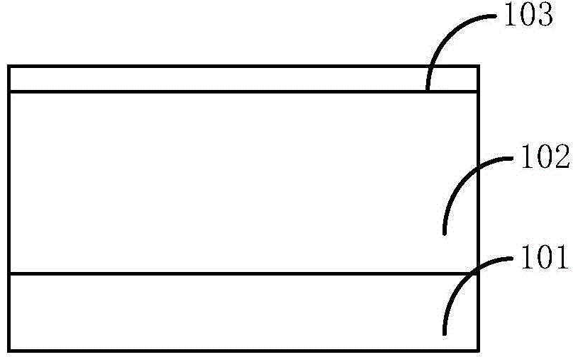
[0046]First, step 201 is performed to provide a semiconductor substrate 201 in which a well region 202 is formed.

[0047] Specifically, refer to Figure 2a , including a semiconductor substrate 201, wherein the semiconductor substrate 201 can be silicon, silicon-on-insulator (SOI), silicon-on-insulator (SSOI), silicon-germanium-on-insulator (S-SiGeOI), silicon-germanium-on-insulator ( SiGeOI) and germanium on insulator (GeOI), etc.

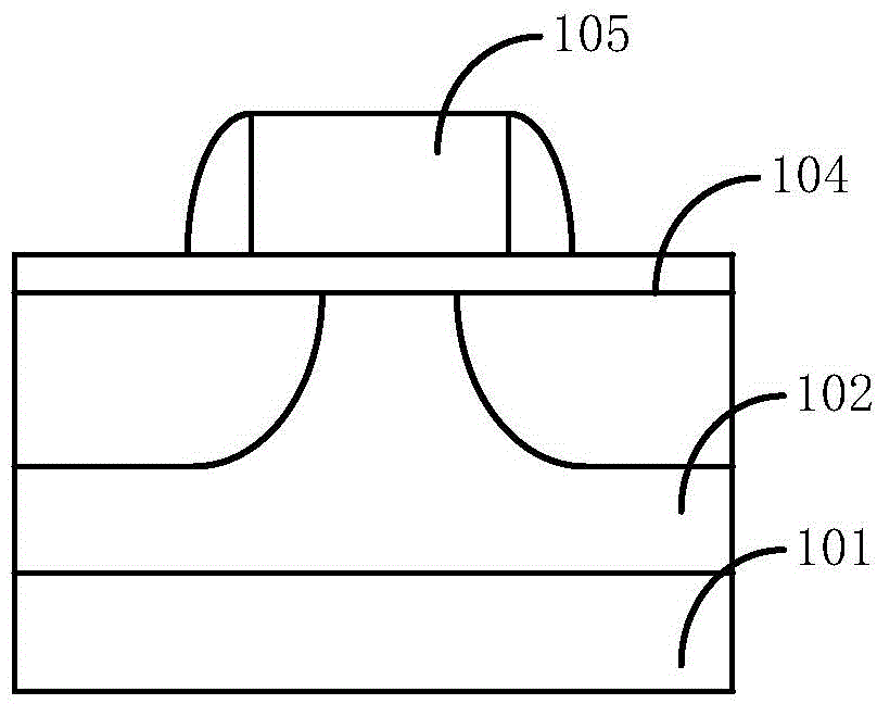
[0048] A well region 202 is formed in the semiconductor substrate 201, which has a first conductivity type. In a specific embodiment of the present invention, the first well region is N+ or P+ doped, for example, N-type dopant (such as phosphorus) is implanted into the semiconductor substrate, and the dopant is driven in by a heat treatment process, thereby forming the N-type well region.

[0049] Before performing ion implantation to form the well region 202, it also includes the step of forming a shielding layer (screen) (not shown in the fig...

Embodiment 2

[0079] As a preferred embodiment, such as Figure 3a-3b As shown, after forming the well region 202 and before forming the drift region, a step of forming a shallow trench isolation structure in the well region 202 is also included.

[0080] A method for forming a shallow trench isolation structure includes the following steps:

[0081] First, a first oxide layer and a first nitride layer are sequentially formed on the semiconductor substrate 201 . The first oxide layer can be obtained by high temperature oxidation, and its thickness can be 100-200 angstroms. The first oxide layer may serve as an isolation layer to protect the semiconductor substrate 301 from damage and contamination. The first nitride layer may be formed by a chemical vapor deposition (CVD) method, a physical vapor deposition (PVD) method, an atomic layer deposition (ALD) method, or the like. As an example, the first nitride layer may be formed by low pressure chemical vapor deposition using ammonia and di...


PUM

PropertyMeasurementUnit
Thicknessaaaaaaaaaa

Abstract

The invention relates to a transverse diffusion semiconductor device and a preparation method thereof. The method comprises the steps of providing a semiconductor substrate, and forming a well region and a drift region in the semiconductor substrate; forming stepped gate dielectric layers on the semiconductor substrate, wherein the gate dielectric layer positioned above a channel region is thinner; forming a gate structure on each of the stepped gate dielectric layers, and executing source and drain injection, so as to form source and drain regions on both sides of each gate structure. According to the semiconductor device, the stepped gate dielectric layers with different heights are formed on the semiconductor substrate, so as to further form the gate structures, and the method is used for increasing the breakdown voltage between drain and source (BVDS) of the device, so that the performance of the device is further improved.

Description

technical field [0001] The invention relates to the field of semiconductors, in particular, the invention relates to a lateral diffusion semiconductor device and a preparation method thereof. Background technique [0002] With the rapid development of the semiconductor industry, PIC (Power Integrated Circuit, power integrated circuit) is continuously used in many fields, such as motor control, flat panel display drive control, computer peripheral drive control, etc., the PIC circuit used Among power devices, DMOS (Double Diffused MOSFET, Double Diffused Metal Oxide Semiconductor Field Effect Transistor) has high operating voltage, simple process, and is easy to be compatible with low-voltage CMOS (Complementary Metal Oxide Semiconductor, Complementary Metal Oxide Semiconductor) circuits in terms of process, etc. characteristics have received widespread attention. [0003] There are two main types of DMOS: vertical double-diffused MOSFET (VDMOS) and lateral double-diffused M...

Claims


Application Information

Patent Timeline
IPC IPC(8): H01L21/336H01L21/28H01L29/78H01L29/423
CPCH01L29/66681H01L29/42368H01L29/7816
Inventor 宋化龙
Owner SEMICON MFG INT (SHANGHAI) CORP
Learn More