A non-parallel plate capacitively coupled plasma chemical vapor deposition method

A capacitive coupling and plasma technology, which is applied in the field of non-parallel plate capacitively coupled plasma chemical vapor deposition, can solve problems such as film defects and substrate damage, and achieve the effects of improving quality, reducing surface damage, and suppressing bombardment

Active Publication Date: 2018-01-05
JIANGNAN UNIV
View PDF3 Cites 0 Cited by
  • Summary
  • Abstract
  • Description
  • Claims
  • Application Information

AI Technical Summary

Problems solved by technology

[0006] Technical problem: The present invention proposes a new thin film deposition technology based on plasma chemical vapor deposition to solve the problem of substrate damage or thin film caused by plasma bombardment of the substrate surface in traditional plasma deposition technologies (PECVD and ICPCVD). Defects and other issues

Method used


Image

  • A non-parallel plate capacitively coupled plasma chemical vapor deposition method
  • A non-parallel plate capacitively coupled plasma chemical vapor deposition method
  • A non-parallel plate capacitively coupled plasma chemical vapor deposition method

Examples


Embodiment Construction

[0019] The present invention will be further described in detail below in conjunction with the accompanying drawings and specific embodiments.

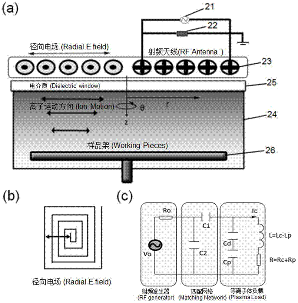
[0020] First of all, for the convenience of explanation, we define the positive z-axis direction passing through the center of the plane spiral coil and perpendicular to the downward direction of the coil, and define the r-direction as the direction perpendicular to the Z-axis. exist figure 2 In (a), when the planar coil 23 is injected with a lower frequency (500kHz) current by the radio frequency generator 21, there are two different electric fields in the discharge space at the same time, which are radial electrostatic fields ( Capacitive coupling) and the eddy electric field (inductive coupling) generated by the change of the magnetic field in the discharge space. In the non-parallel plate capacitively coupled plasma discharge mode, the RF input power is lower, resulting in lower coil current and thicker plasma shell, so that the...


PUM

PropertyMeasurementUnit
diameteraaaaaaaaaa
thicknessaaaaaaaaaa

Abstract

The invention relates to a thin film deposition method, especially a non-parallel plate capacitively coupled plasma chemical vapor deposition method, which comprises a planar rectangular helical inductance antenna, a low-frequency power generator, an impedance matching network, a columnar vacuum chamber, quartz glass and a substrate holder. The present invention realizes the capacitively coupled stable discharge in the vacuum chamber by controlling the radio frequency input power and tuning the matching capacitance: the plasma density is low, and the radial electrostatic field parallel to the substrate surface established by the potential difference at both ends of the coil plays a leading role , so that the movement of positive ions is constrained in a direction parallel to the substrate surface. Therefore, the present invention starts from two aspects, that is, reducing the plasma density and restricting the movement direction of the positive ions, which can significantly suppress the bombardment of the positive ions on the surface of the film during the chemical vapor deposition process and reduce surface damage. This system can be used to prepare various passivation layers necessary for high-efficiency crystalline silicon solar cells, such as amorphous silicon and amorphous silicon nitride.

Description

technical field [0001] The invention relates to a thin film deposition method based on plasma chemical vapor deposition, which belongs to the technical field of plasma chemical vapor deposition methods, and can be applied to various passivation thin layers of high-efficiency crystalline silicon solar cells, including amorphous silicon, amorphous nitride Preparation of silicon, amorphous silicon dioxide and amorphous silicon carbide, etc. Background technique [0002] A plasma is a collection of freely charged particles moving randomly. From a macroscopic point of view, plasma is electrically neutral. The simplest way to form it is to drive the two plates through a radio frequency voltage source, so that the low-pressure gas between the plates produces a discharge phenomenon. When the current flows from one plate to the other, the gas is "broken down" to generate plasma . Plasma discharges can produce chemically active species and thus enable the fabrication of materials w...

Claims


Application Information

Patent Timeline
Patent Type & Authority Patents(China)
IPC IPC(8): C23C16/505
Inventor 肖少庆张学成顾晓峰丁荣
Owner JIANGNAN UNIV
Why Eureka
Try Eureka