

Manufacturing method of metal grating on silicon-based heterojunction cell
A technology of heterojunction batteries and metal grid lines, which is applied in metal material coating technology, circuits, electrical components, etc., can solve problems such as weak welding ability, high cost, and difficult process, and achieve increased adhesion and easy The effect of welding
- Summary
- Abstract
- Description
- Claims
- Application Information
AI Technical Summary
Problems solved by technology
Method used
Image

Examples
Embodiment Construction
[0034] In order to make the object, technical solution and advantages of the present invention clearer, the present invention will be further described in detail below in conjunction with the accompanying drawings and embodiments. It should be understood that the specific embodiments described here are only used to explain the present invention, not to limit the present invention.
[0035] The invention provides a method for manufacturing metal grid lines on a silicon-based heterojunction solar cell. The method mainly realizes the production of metal grid lines by electroplating, and mainly includes the following steps:
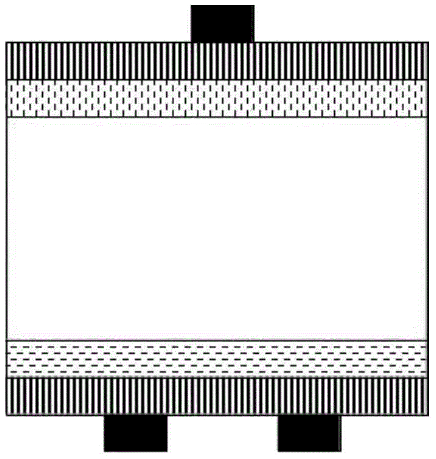
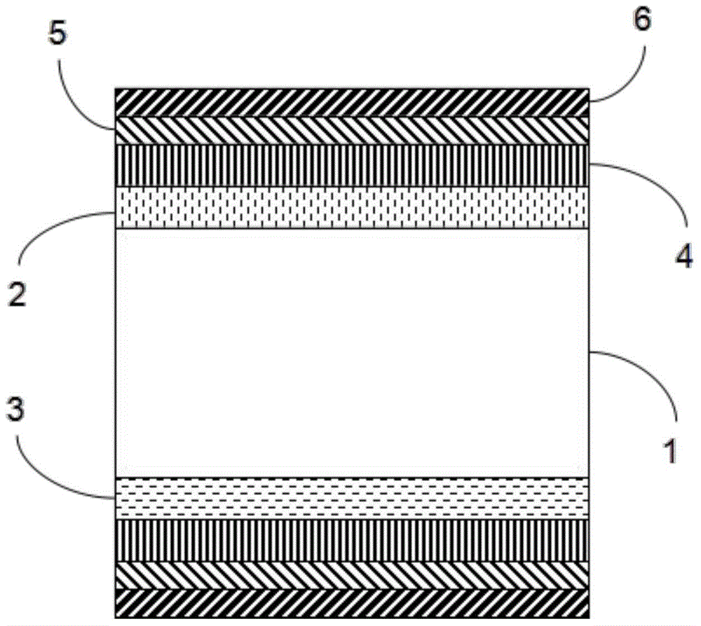
[0036] In the first step, a P-type amorphous silicon film layer 2 is deposited on one side of the N-type silicon wafer 1 with an uneven surface after being etched by an alkaline or acidic solution, and an N-type amorphous silicon film is deposited on the other side by CVD. Thin film layer 3, wherein the reflectivity of the surface of the silicon wafer 1 is le...
PUM
| Property | Measurement | Unit |
|---|---|---|
| thickness | aaaaa | aaaaa |
| thickness | aaaaa | aaaaa |
| thickness | aaaaa | aaaaa |
Abstract
Description
Claims
Application Information