
Method for manufacturing CZTS thin film solar cell absorbing layer

A thin-film solar cell and absorption layer technology, which is applied to circuits, photovoltaic power generation, electrical components, etc., can solve the problems of difficult to form CZTS thin-film solar cells industrialized production, low-quality specific power of thin-film solar cells, and narrowing the use range of batteries, etc. Achieve the effect of improving electrical performance, improving conversion efficiency and good uniformity

Inactive Publication Date: 2015-06-17
CHINA ELECTRONIC TECH GRP CORP NO 18 RES INST
View PDF2 Cites 4 Cited by
  • Summary
  • Abstract
  • Description
  • Claims
  • Application Information

AI Technical Summary

Problems solved by technology

[0003] The currently known methods for preparing the absorber layer of CZTS thin-film solar cells mainly include: first preparing a layer of precursors containing Cu, Zn, and Sn on the soda-lime glass substrate, and then performing post-selenization and annealing to obtain CZTS thin-film solar cells Absorbing layer, due to the difficulty of post-selenization and annealing treatment, the reaction process is not easy to control, the manufacturing process is complicated, and the repeatability is poor. range, and it is difficult to form the industrial production of CZTS thin film solar cells

Method used


Image

  • Method for manufacturing CZTS thin film solar cell absorbing layer

Examples


preparation example Construction

[0020] The preparation method of the CZTS thin film solar cell absorbing layer is characterized in that it comprises the following preparation steps:

[0021] Step 1: Fix the flexible substrate with the film-coated side facing down under the sample holder below the rotating shaft on the top wall of the vacuum evaporation chamber, and a movable substrate baffle is placed under the flexible substrate; the top of the sample holder Fix a thermocouple, and there is a substrate heater on the rotating shaft above the thermocouple; the Cu evaporation source, Zn evaporation source, NaF evaporation source, Sn evaporation source and Se evaporation source are placed in the vacuum evaporation chamber at any angle and height. Among the adjusted five wedge-shaped evaporation source bases, the distance from the top of the Cu evaporation source, Zn evaporation source, NaF evaporation, and Sn evaporation source to the center of the bottom of the substrate is ≤ 30cm, and the distance from the top...

Embodiment

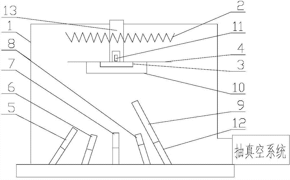
[0027] Step 1: If figure 1 As shown, a vacuum evaporation chamber 1 is set on the top wall to rotate the rotating shaft 13 through the outside; the 10×10cm 2 The PI flexible substrate 3 is coated with a 500-800nm ​​Mo back electrode on one side, and the Mo back electrode on the flexible substrate is fixed on the bottom of the rotating shaft. Below, below the flexible substrate, there is a substrate baffle plate 10 installed under the sample holder and can be opened and closed in the vacuum evaporation chamber; a thermocouple 11 is fixed above the sample holder, and the rotation axis above the thermocouple is fixed horizontally to The serpentine coiled furnace wire is used as the substrate heater 2; there are five evaporation source bases 12 arranged in a ring at the bottom of the vacuum evaporation chamber, and the angle and height can be adjusted, each with a Cu evaporation source 5 and a Zn evaporation source with a heater Source 6, NaF evaporation source 7, Sn evaporation ...


PUM


Abstract

The invention relates to a method for manufacturing a CZTS thin film solar cell absorbing layer. The method includes the steps that Cu, Zn, Sn, Se and NaF are co-evaporated on the lower face of a flexible substrate, so that a copper-rich CZTS thin film is formed; a substrate baffle is closed, after Cu and NaF are cooled, the substrate baffle is opened, Zn, Sn and Se are co-evaporated on the lower face of the flexible substrate, and the substrate baffle is closed; after Zn is cooled, the substrate baffle is opened and the substrate is cooled in the atmosphere of Sn and Se; the CZTS thin film solar cell absorbing layer is formed on the flexible substrate. By the adoption of the method, flexible PI serves as the substrate, a co-evaporation method is adopted, the evaporation temperature, the evaporation time, and the evaporation sequence and the like of the evaporation sources of Cu, Zn, Sn and Se are controlled, so that a reaction route and composition are controlled, the post-selenylation and annealing processes are avoided, the manufactured CZTS thin film solar cell absorbing layer is high in crystallization quality and good in evenness, the manufacturing process is simple, repeatability is high, and the industrialization of CZTS thin film solar cells is facilitated.

Description

technical field [0001] The invention belongs to the technical field of thin film solar cell production, in particular to a method for preparing an absorbing layer of a CZTS thin film solar cell. Background technique [0002] Thin-film solar cells, especially CIGS thin-film solar cells, have developed rapidly in recent years. At present, the laboratory conversion efficiency of CIGS thin film solar cells has reached 20.4%, and its industrialization process is also being accelerated. However, the key elements In and Ga in the absorbing layer of CIGS thin-film solar cells are limited, and the price is relatively high, which limits the large-scale industrialization of CIGS thin-film solar cells. CZTS (copper zinc tin sulfur (selenium), that is, Cu2ZnSn (S, Se) 4 ) film and CIGS film have similar photoelectric characteristics, and CZTS film replaces In and Ga in CIGS film with Zn and Sn elements with abundant reserves and low price, which further reduces the cost of film prepara...

Claims


Application Information

Patent Timeline
Patent Type & Authority Applications(China)
IPC IPC(8): H01L31/18
CPCH01L21/02422H01L21/02568H01L21/0257H01L21/02631H01L31/0326H01L31/0327Y02E10/50Y02P70/50
Inventor 王胜利杨亦桐杨立李微赵彦民乔在祥
Owner CHINA ELECTRONIC TECH GRP CORP NO 18 RES INST
Learn More