Semiconductor device and manufacturing method thereof

A semiconductor and device technology, applied in the display field, can solve the problems of reduced voltage withstand performance of capacitors, and achieve the effect of solving the problem of reduced voltage withstand performance, excellent voltage withstand performance, and reducing production costs

Active Publication Date: 2015-06-17
CHENGDU VISTAR OPTEOLECTRONICS CO LTD
View PDF5 Cites 3 Cited by
  • Summary
  • Abstract
  • Description
  • Claims
  • Application Information

AI Technical Summary

Problems solved by technology

[0007] Therefore, what the present invention aims to solve is the problem that the manufacturing method of the semiconductor device in the existing active matrix organic light-emitting display device easily leads to a reduction in the withstand voltage performance of the capacitor, and provides a method for preparing a semiconductor device that does not affect the withstand voltage performance of the capacitor and semiconductor devices prepared by the method

Method used


Image

  • Semiconductor device and manufacturing method thereof
  • Semiconductor device and manufacturing method thereof
  • Semiconductor device and manufacturing method thereof

Examples


Embodiment

[0040] This embodiment provides a method for preparing a semiconductor device and a semiconductor device prepared therefor, including the following steps:

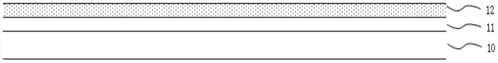
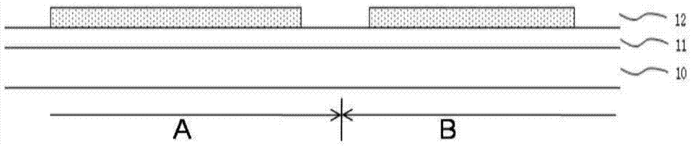
[0041] S1, such as figure 2 As shown, a semiconductor layer 12 is formed on a substrate 10 including a thin film transistor region A and a capacitor region B; image 3 As shown, the semiconductor layer 12 is patterned by photolithography and dry etching processes to form island-shaped patterns in the thin film transistor region A and capacitor region B respectively.

[0042] The substrate 10 is selected from but not limited to a glass substrate, a polymer substrate or a metal substrate, all of which can achieve the purpose of the present invention and belong to the protection scope of the present invention. In this embodiment, a glass substrate is preferred; the substrate 10 is divided into a thin film transistor region A and a capacitor region B, but there is no clear boundary between them. The thin film transistor is f...


PUM


Abstract

The invention provides a semiconductor device manufacturing method. The technology of directly injecting high-concentration impurity ions to a semiconductor layer is adopted, injection of the high-concentration impurity ions through a capacitor dielectric layer can be avoided, and influences on the capacitor dielectric layer are thus reduced. On the premise of not increasing the technological steps, the problems that voltage-resisting performance of the capacitor is reduces as the capacitor dielectric layer is damaged can be effectively solved, the yield of the semiconductor devices is improved, and the production cost is greatly reduced. According to the semiconductor device provided by the invention, the capacitor has excellent voltage-resisting performance, threshold voltage of a thin film transistor has a small shift value, the manufacturing method is simple, and large-scale industrial production can be realized.

Description

technical field [0001] The invention relates to the field of display technology, in particular to a method for preparing a semiconductor device in an active matrix organic electroluminescent display device and the semiconductor device prepared by the method. Background technique [0002] Organic Light-Emitting Diode (English full name Organic Light-Emitting Diode, referred to as OLED) is an active light-emitting device, which has the advantages of high contrast, wide viewing angle, and low power consumption. It is currently one of the most concerned technologies in flat panel display technology. [0003] The active matrix organic light-emitting display device (English full name Active Matrix organic lighting emitting display, referred to as AMOLED) uses a thin film transistor (English full name Thin Film Transistor, referred to as TFT), with a capacitor to store signals to control the brightness and gray scale of organic light-emitting diodes. performance display device. Ea...

Claims


Application Information

Patent Timeline
Patent Type & Authority Applications(China)
IPC IPC(8): H01L51/56H01L51/52H01L27/32
Inventor 陈浩
Owner CHENGDU VISTAR OPTEOLECTRONICS CO LTD
Why Eureka
Try Eureka