Manufacturing method of metal mesh conducting film, metal mesh conducting film and touch panel
A metal grid and manufacturing method technology, applied in electrical digital data processing, data processing input/output process, instruments, etc., can solve the problems of high cost, high ITO resistance, many steps, etc., to enhance adhesion, High response speed, low cost effect
- Summary
- Abstract
- Description
- Claims
- Application Information
AI Technical Summary
Problems solved by technology
Method used
Image

Examples
Embodiment 1
[0054] The manufacturing method of the metal grid conductive film provided in this embodiment includes the following steps:
[0055] S10: forming a metallic ink coating on the substrate.
[0056] Prepare the nano-copper ink coating and CPI film (transparent polyimide film), and apply the nano-copper ink to the CPI film by slit coating. The nano-copper ink coating is composed of copper nanoparticles (average particle size is 45nm), dispersant (manufactured by HUNTSMAN Company of the United States), 1,2-propanediol and propylene glycol monobutyl ether, wherein the content of copper nanoparticles is about 20wt%. The thickness of the CPI film is 50 μm.
[0057] S20: Baking the metallic ink coating.
[0058] Transfer the CPI film coated with nano-copper ink to a hot air drying oven and bake at 100°C for 30 minutes to remove the solvent, and obtain a layer of nano-copper ink coating with a dry film thickness of about 1 μm on the surface of the CPI film.
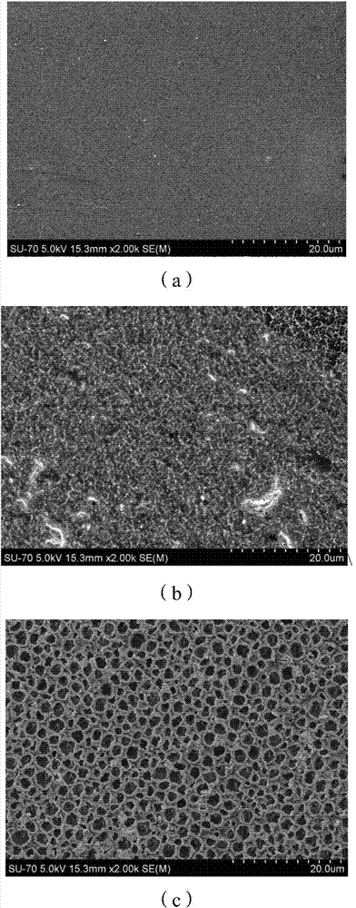
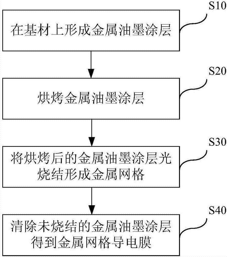
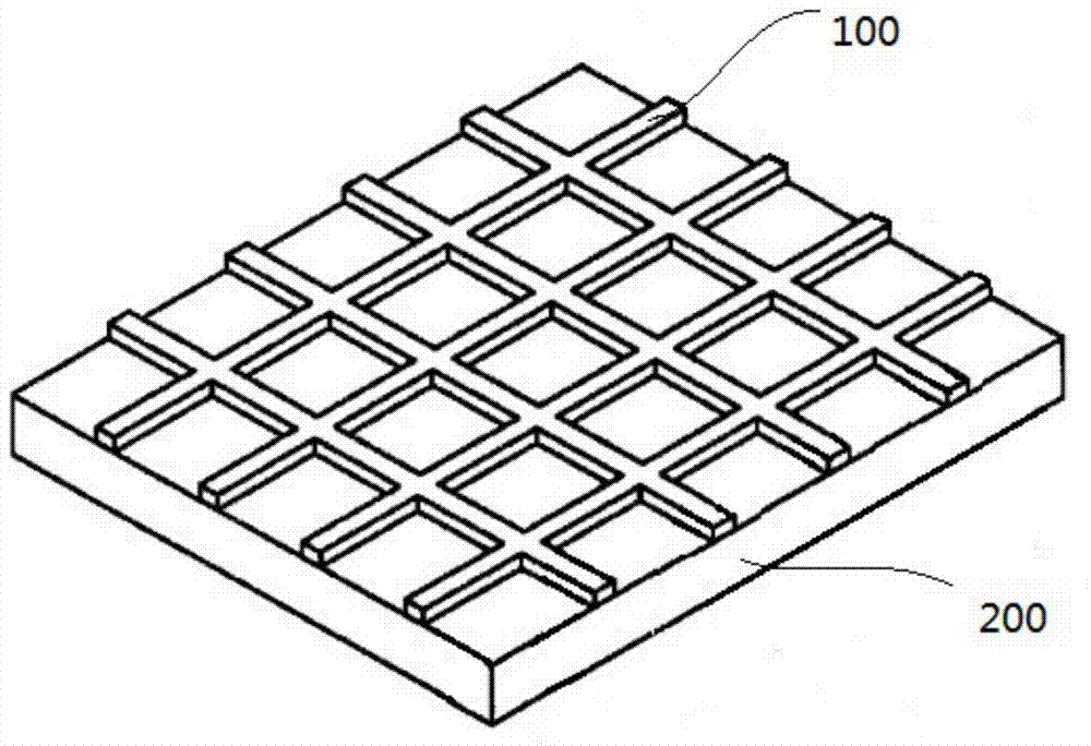
[0059] S30: Photo-sint...
Embodiment 2
[0064] The manufacturing method of the metal grid conductive film provided in this embodiment includes the following steps:
[0065] S10: forming a metallic ink coating on the substrate.
[0066] Prepare the nano-copper ink coating and the CPI film, and apply the nano-copper ink to the CPI film by spin coating. The nano-copper ink coating is composed of copper nanoparticles (average particle size is 45nm), dispersant (manufactured by HUNTSMAN Company of the United States), 1,2-propanediol and propylene glycol monobutyl ether, wherein the content of copper nanoparticles is about 20wt%. The thickness of the CPI film is 50 μm.
[0067] S20: Baking the metallic ink coating.
[0068] Transfer the CPI film coated with nano-copper ink to a hot air drying oven and bake at 80°C for 30 minutes to remove the solvent, and obtain a layer of nano-copper ink coating with a dry film thickness of about 0.5 μm on the surface of the CPI film.
[0069] S30: Photo-sintering the baked metal in...
Embodiment 3
[0074] The manufacturing method of the metal grid conductive film provided in this embodiment includes the following steps:
[0075] S10: forming a metallic ink coating on the substrate.
[0076] Prepare the nano-silver ink coating and the PEN film, and apply the nano-silver ink to the PEN film by slit coating. Nano-silver ink coating consists of silver nanoparticles (average particle size is 20nm), dispersant (manufactured by U.S. HUNTSMAN company), 1,2-propanediol and propylene glycol monobutyl ether, wherein the content of silver nanoparticles is about 20wt%. The thickness of the PEN film was 188 μm.
[0077] S20: Baking the metallic ink coating.
[0078] Transfer the PEN film coated with nano-silver ink to a hot air drying oven and bake at 80°C for 30 minutes to remove the solvent, and obtain a layer of nano-silver ink coating with a dry film thickness of about 2 μm on the surface of the PEN film.
[0079] S30: Photo-sintering the baked metal ink coating to form a met...
PUM
| Property | Measurement | Unit |
|---|---|---|
| Pulse width | aaaaa | aaaaa |
| Dry film thickness | aaaaa | aaaaa |
| Particle size | aaaaa | aaaaa |
Abstract
Description
Claims
Application Information
 - Generate Ideas
- Intellectual Property
- Life Sciences
- Materials
- Tech Scout
- Unparalleled Data Quality
- Higher Quality Content
- 60% Fewer Hallucinations
Browse by: Latest US Patents, China's latest patents, Technical Efficacy Thesaurus, Application Domain, Technology Topic, Popular Technical Reports.
© 2025 PatSnap. All rights reserved.Legal|Privacy policy|Modern Slavery Act Transparency Statement|Sitemap|About US| Contact US: help@patsnap.com