A kind of thin film transistor and its manufacturing method

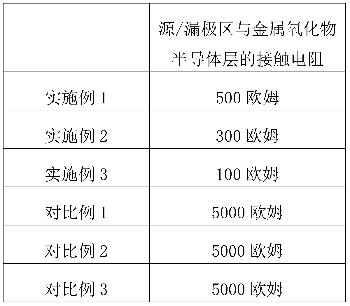
A technology of thin film transistors and manufacturing methods, which is applied in the field of organic light-emitting display devices, can solve the problems of large contact resistance and small contact resistance of semiconductor layers and source/drain electrode layers, and reduce contact resistance, save machine time and cost, and reduce The effect of one-time film forming process

Active Publication Date: 2018-11-13
CHENGDU VISTAR OPTEOLECTRONICS CO LTD
View PDF5 Cites 0 Cited by
  • Summary
  • Abstract
  • Description
  • Claims
  • Application Information

AI Technical Summary

Problems solved by technology

[0006] For this reason, what the present invention is to solve is the problem that the contact resistance between the semiconductor layer and the source / drain electrode layer of the top-gate type metal oxide thin film transistor is relatively large in the prior art, thereby proposing that the metal oxide semiconductor layer and the source / drain electrode layer contact Thin film transistor with small resistance and manufacturing method thereof

Method used


Image

  • A kind of thin film transistor and its manufacturing method
  • A kind of thin film transistor and its manufacturing method
  • A kind of thin film transistor and its manufacturing method

Examples


Embodiment 1

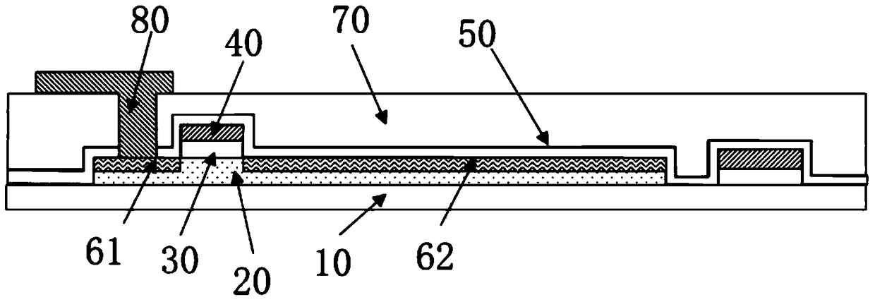
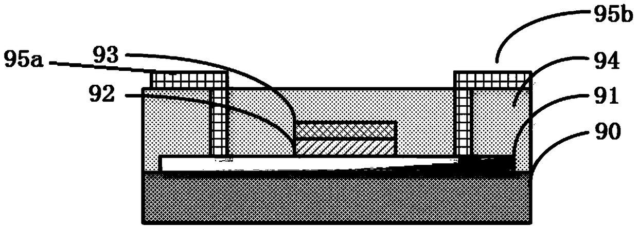
[0043] This embodiment provides a thin film transistor, such as figure 2As shown, it includes a metal oxide semiconductor layer 91, a first insulating layer 92, a gate layer 93, a second insulating layer 94 stacked on a substrate 90 in sequence, and a source electrode 95a and a drain electrode arranged at both ends of the second insulating layer. Pole 95b.

[0044] The metal oxide semiconductor layer 91 can be selected from but not limited to indium gallium zinc oxide (Indium Gallium Zinc Oxide referred to as IGZO), indium zinc oxide (Indium Zinc Oxide referred to as IZO), aluminum doped indium zinc oxide (Al-IZO ) and other materials, this embodiment is preferably IGZO material, its thickness can be 20nm-400nm, this embodiment is preferably 300nm.

[0045] The first insulating layer 92 is a metal oxide layer obtained after oxidation of a metal layer. The metal oxide layer has insulating properties. The metal layer can be selected from but not limited to one of Al, Zn, Fe, a...

Embodiment 2

[0055] On the basis of Embodiment 1, the structure of the thin film transistor in this embodiment is as follows figure 2 shown.

[0056] Wherein, the first insulating layer 92 can be selected from one or more stacked layers of directly formed insulating metal oxide layer, silicon nitride layer or silicon oxide layer. In this embodiment, Al 2 o 3 The thickness of the layer may be 50nm-350nm, preferably 150nm in this embodiment.

[0057] The second insulating layer 94 is a metal oxide layer obtained after oxidation of the metal layer. The metal oxide layer has insulating properties. The metal layer can be selected from but not limited to Al, Zn, Fe, Cu. One or more combinations, this embodiment is preferably Al obtained by oxidation of the Al layer 2 o 3 The thickness of the layer may be 100nm-500nm, preferably 400nm in this embodiment. The second insulating layer 94 is directly formed on the first insulating layer 92 and covers the gate layer 93; the second insulating lay...

Embodiment 3

[0066] On the basis of Embodiment 1 or Embodiment 2, the structure of the thin film transistor in this embodiment is as follows figure 2 shown.

[0067] Wherein, the first insulating layer 92 is a metal oxide layer obtained after the metal layer is oxidized. The metal oxide layer has insulating properties. The metal layer can be selected from but not limited to one of Al, Zn, Fe, and Cu. A combination of one or more, this embodiment is preferably Al obtained by oxidation of the Al layer 2 o 3 The thickness of the layer may be 50nm-350nm, preferably 150nm in this embodiment.

[0068] The second insulating layer 94 is a metal oxide layer obtained after oxidation of the metal layer. The metal oxide layer has insulating properties. The metal layer can be selected from but not limited to one of Al, Zn, Fe, Cu, or A variety of combinations, this embodiment is preferably Al obtained by oxidation of the Al layer 2 o 3 The thickness of the layer may be 100nm-500nm, preferably 400...


PUM

PropertyMeasurementUnit
thicknessaaaaaaaaaa
thicknessaaaaaaaaaa
thicknessaaaaaaaaaa

Abstract

The invention relates to a thin film transistor. The thin film transistor comprises a metal-oxide semiconductor layer, a first insulating layer, a grid layer, a second insulating layer and a source / drain electrode layer, wherein the metal-oxide semiconductor layer, the first insulating layer, the grid layer, the second insulating layer and the source / drain electrode layer are laminated on a substrate respectively. The first insulating layer and / or the second insulating layer are / is (a) metal oxide layer(s) obtained by oxidation of metal layer(s), and the metal layers have insulating performance. In the oxidation process, the metal layer absorbs part of oxygen ions of the metal-oxide semiconductor layer, the oxygen content of the metal-oxide semiconductor layer can be reduced, the conductive performance of the metal-oxide semiconductor layer is improved, and the contact resistance between the metal-oxide semiconductor layer and the source / drain electrode layer is effectively reduced. The invention also provides a manufacture method of the thin film transistor, the contact resistance between the metal-oxide semiconductor layer and the source / drain electrode layer is effectively reduced by oxidation of the metal layer, technology is simple and the production cost is greatly reduced.

Description

technical field [0001] The invention relates to an organic light-emitting display device. Specifically, it relates to a thin film transistor and a manufacturing method thereof. Background technique [0002] Organic electroluminescence refers to the phenomenon that organic light-emitting materials emit light under the excitation of electric current or electric field. Organic Lighting Emitting Display (OLED for short) is different from traditional liquid crystal display (Liquid Crystal Display, LCD for short) in display mode. OLED has the advantages of thin thickness, wide viewing angle, high contrast, fast response, low power consumption, and flexibility. It is one of the most concerned technologies in flat panel display technology, and has become the most promising next-generation flat panel to replace LCD. display technology. [0003] As one of the key devices of organic light-emitting displays, the performance of thin-film transistors (Thin-film transistors, referred to...

Claims


Application Information

Patent Timeline
Patent Type & Authority Patents(China)
IPC IPC(8): H01L29/786H01L21/336
CPCH01L29/66742H01L29/78684
Inventor 敖伟朱少鹏刘金强罗志忠习王锋
Owner CHENGDU VISTAR OPTEOLECTRONICS CO LTD
Why Eureka
Try Eureka