Self-excited spinning single-electron electromagnetic field effect transistor, preparation method and application

An electromagnetic field and transistor technology, applied in the field of self-excited spin single-electron field effect transistors, can solve problems such as obstacles to the development of quantum computers

Active Publication Date: 2015-07-15
HUBEI UNIV OF TECH
View PDF5 Cites 19 Cited by
  • Summary
  • Abstract
  • Description
  • Claims
  • Application Information

AI Technical Summary

Problems solved by technology

Moreover, because this effect occurs at low temperatures

Method used


Image

  • Self-excited spinning single-electron electromagnetic field effect transistor, preparation method and application
  • Self-excited spinning single-electron electromagnetic field effect transistor, preparation method and application
  • Self-excited spinning single-electron electromagnetic field effect transistor, preparation method and application

Examples


Embodiment 1

[0086] 1. Material growth

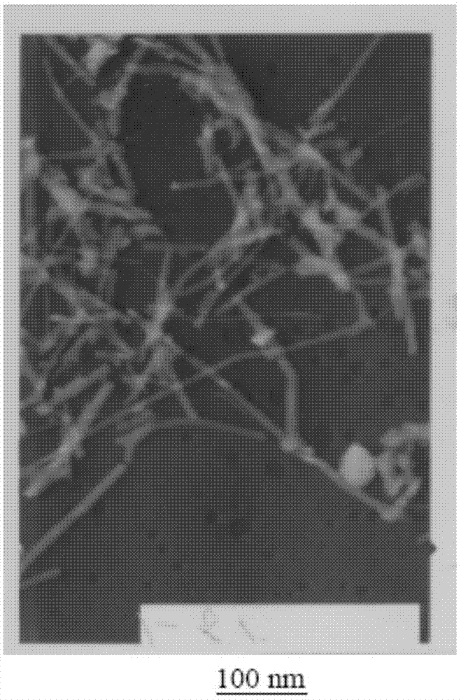
[0087] Preparation of polytype 4H-SiC / 6H-SiC silicon carbide nanowires.

[0088] The SOI silicon wafer is cleaned by ultrasonic oscillation with an electronic cleaning agent, and silicon carbide is deposited on the SOI silicon wafer by using a high power density enhanced chemical vapor deposition device (PECVD device) with the SOI silicon wafer as the substrate. Compared with the deposition of amorphous silicon thin films, the deposition of silicon carbide requires a stronger plasma, which is conducive to the formation of silicon carbide crystal nuclei and the crystallization of amorphous particles; , an alternating electromagnetic field is required during the deposition process.

[0089] In the reaction chamber of the PECVD device, the solid mixed material of Ni, Mn, Co, Fe, Cr, Hf, Nd, V and Al is used as the catalyst, and the preparation method of the above solid mixed material is: according to (0.1~1): (0.1~ 1): (0.1~1): (0.1~1): (0.1~1): (0.1...

Embodiment 2

[0099] Preparation of hexagonal polytype silicon carbide nanowires.

[0100] With the SOI silicon wafer substrate, a high power density enhanced chemical vapor deposition device (PECVD device) is used to deposit silicon carbide on the SOI silicon wafer. Put the substrate into the reaction chamber of the PECVD device, use the solid-state mixed material of magnetic metal Mn and Ni as the catalyst, and dilute trichlorosilane (HSiCl 3 ) and high hydrogen diluted acetylene (C 2 h 2 ) is the reaction source gas, and at the same time pass into high hydrogen to dilute BH 3 The gas is used as P-type doping, and the volume flow rate of the mixed gas should comply with: Q HSiCl3 / (Q HSiCl3 +Q CH2 )=0.01~0.4, Q HSiCl3 / (Q HSiCl3 +Q CH2 +Q BH3 )=0.01~0.3, Q HSiCl3 , Q CH2 , Q BH3 They are high hydrogen diluted trichlorosilane, high hydrogen diluted acetylene, high hydrogen diluted BH in the reaction chamber 3 volume flow. The vacuum degree in the reaction chamber is 1-10 -4 ...

Embodiment 3

[0102] Preparation of cubic lattice silicon carbide nanowires.

[0103] With the SOI silicon wafer substrate, a high power density enhanced chemical vapor deposition device (PECVD device) is used to deposit silicon carbide on the SOI silicon wafer. Put the substrate into the reaction chamber of the PECVD device, use the solid mixed material of magnetic metal Co and Fe as the catalyst, and dilute trichlorosilane (HSiCl 3 ) and high hydrogen diluted acetylene (C 2 h 2 ) is the reaction source gas, while feeding high hydrogen to dilute the PH 3 The gas is used as P-type doping, and the volume flow rate of the mixed gas should comply with: Q HSiCl3 / (Q HSiCl3 +Q CH2 )=0.01~0.4, Q HSiCl3 / (Q HSiCl3 +Q CH2 +Q PH3 )=0.01~0.3, Q HSiCl3 , Q CH2 , Q PH3 Respectively high hydrogen diluted trichlorosilane, high hydrogen release acetylene, high hydrogen diluted PH in the reaction chamber 3 volume flow. The vacuum degree in the reaction chamber is 1-10 -4 Torr, using the tech...


PUM

PropertyMeasurementUnit
Curie temperatureaaaaaaaaaa

Abstract

The invention discloses a self-excited spinning single-electron electromagnetic field effect transistor, a preparation method and the application. The electromagnetic field effect transistor comprises a base plate, a source electrode, a drain electrode, a gate electrode and a nanowire active area. The source electrode, the drain electrode and the gate electrode are arranged on the base plate. The nanowire active area is a current channel between the source electrode and the drain electrode, and the nanowire active area is polymorphic silicon carbide nanowires mingling with magnetic metals. According to the self-excited spinning single-electron electromagnetic field effect transistor, the preparation method and the application, and the indoor temperature can realize a single-electron coulomb block effect and a single-electron tunneling effect; at the same time, when the single-electron coulomb block effect and the single-electron tunneling effect are achieved, the single electron oscillation generates a variable electric field, and the variable electric field generates a magnetic field; under the condition that drain voltage replenishes energy, multi-structure electromagnetic oscillation can be presented, and pA-grade single-electron spinning current is generated. The self-excited spinning single-electron electromagnetic field effect transistor can be used as component for generating, converting, transferring and storing of quantum information.

Description

technical field [0001] The invention belongs to the technical field of self-excited spin single-electron field-effect transistors, and in particular relates to a self-excited spin single-electron self-excited electromagnetic field-effect transistor of a nanowire dilute magnetic semiconductor heterojunction, a preparation method and an application. Background technique [0002] At present, nanowire semiconductor heterojunction single-electron devices are based on Coulomb blocking effect and single electron tunneling (K.K.Likharev.Correlated discrete transfer of single electrons in ultrasmall tunnel junctions".IBM J.Res.Develop.Vol .32, p.144,1989). This single-electron device can theoretically minimize energy consumption, and because it is a single-electron movement, its speed can be very high. However, research on single-electron devices has long focused on Due to the blocking and tunneling of single charges, the device effect caused by electromagnetic induction generated du...

Claims


Application Information

Patent Timeline
IPC IPC(8): H01L29/66H01L43/06
CPCH01L29/66H10N52/101H10N50/85H10N50/01
Inventor 张洪涛
Owner HUBEI UNIV OF TECH
Why Eureka
Try Eureka