Flexible micro pressure sensor and preparation method thereof
A micro pressure sensor, flexible technology, applied in the direction of instruments, microstructure technology, electric solid devices, etc., can solve the problems of reducing sensor sensitivity, limiting the wide application of sensors, limited deformation, etc., achieving low cost, good flexibility and good stability Effect
- Summary
- Abstract
- Description
- Claims
- Application Information
AI Technical Summary
Problems solved by technology
Method used
Image
Examples
preparation example Construction
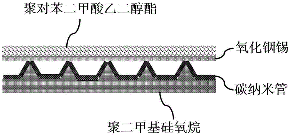
[0031] A method for preparing a flexible micro pressure sensor includes the following steps:
[0032] Step 1: Firstly obtain a square array by photolithography, then use BOE solution and KOH solution to etch a silicon template with a regular quadrangular pyramid microstructure, and treat the silicon template on trimethylchlorosilane for 4h; the KOH solution is KOH , Isopropanol and water mixture, where H 2 The mass ratio of O, KOH and isopropanol is 2:1:2, and the solution needs to be stirred magnetically when etching in the KOH solution;
[0033] Step 2: Mix the polydimethylsiloxane and curing agent uniformly at a mass ratio of 10:1, and put them in a vacuum chamber for vacuum treatment to remove air bubbles;
[0034] Step 3: Drop the mixed droplets of polydimethylsiloxane and curing agent processed in step 2 on the silicon template with regular quadrangular pyramid microstructure obtained in step 1, and put it in a vacuum chamber to vacuum; take it out and heat it to make PDMS cur...
Embodiment
[0038] The present invention also provides a method for preparing a flexible and transparent micro pressure sensor based on carbon nanotubes, which includes the following steps:
[0039] Step 1: Use a silicon wafer with a thickness of 500μm and a layer of silicon dioxide of 300nm on the surface as a substrate to clean the silicon wafer; obtain an array of squares with a side length of 10μm on the silicon dioxide surface by photolithography, adjacent to the square The center distance is 20μm (square silica bare drain); BOE solution (mole ratio NH 4 F: HF=6:1) Etch the above-mentioned substrate at room temperature for 5 minutes to remove the exposed silicon dioxide layer, then put the substrate in acetone to remove the photoresist; put the substrate in KOH solution (quality Than H 2 O: KOH: Isopropanol = 2:1: 2), heat the water bath to 75°C, and etch for 15 min under stirring conditions to obtain a silicon template with a regular quadrangular pyramid microstructure; place the prepar...
PUM
| Property | Measurement | Unit |
|---|---|---|
| thickness | aaaaa | aaaaa |
Abstract
Description
Claims
Application Information


