Tunneling field effect device for channel potential barrier height control

A technology of tunneling field effect and barrier height, which is applied in the field of tunneling field effect devices, can solve the problem of not being lower than that, and achieve the effects of improving performance, reducing size, and promoting development

Inactive Publication Date: 2015-09-02
WUHAN UNIV
View PDF2 Cites 3 Cited by
  • Summary
  • Abstract
  • Description
  • Claims
  • Application Information

AI Technical Summary

Problems solved by technology

The traditional metal-oxide-semiconductor field-effect device belongs to the channel barrier height-controlled structure, which has a large on-state current, but its carriers are based on thermal excitation, and its subthreshold slope cannot be lower than 60 mV / dec at room temperature. physical limit

Method used


Image

  • Tunneling field effect device for channel potential barrier height control
  • Tunneling field effect device for channel potential barrier height control
  • Tunneling field effect device for channel potential barrier height control

Examples


Embodiment 1

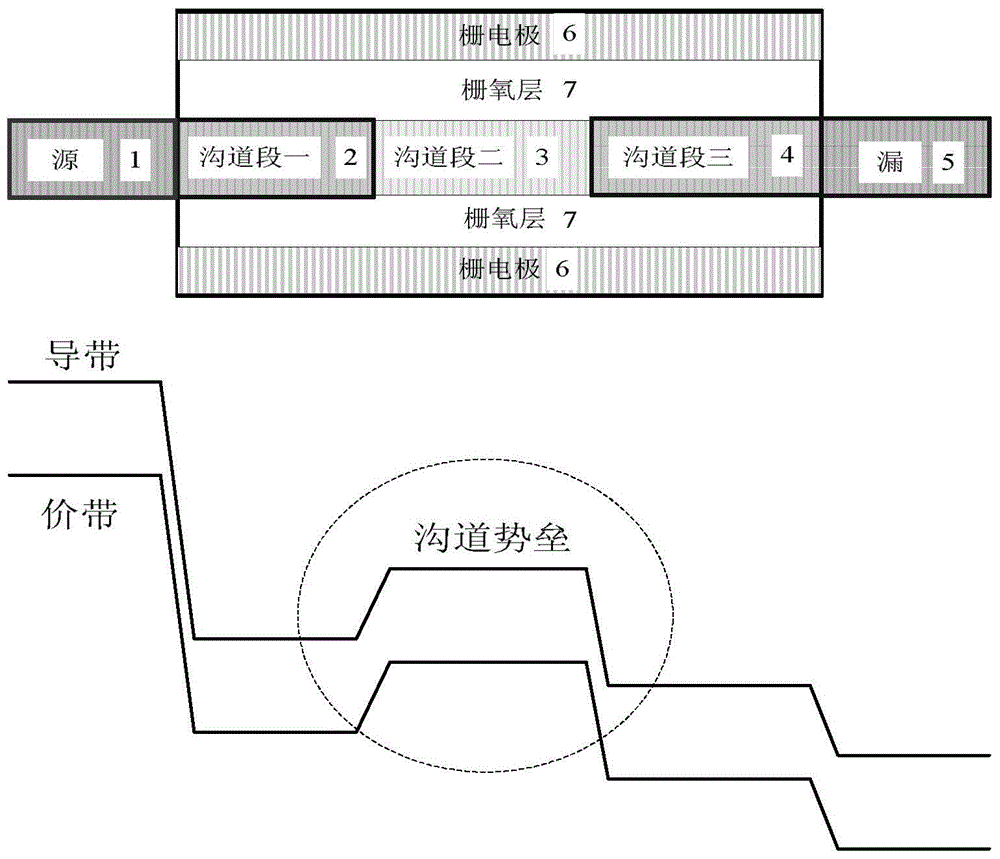
[0037] Example 1: The channel length is 60 nanometers, the source and drain lengths are 20 nanometers each, and the multi-stage doped channel barrier height controls the energy band structure of the tunneling field effect device, which changes with the gate voltage.

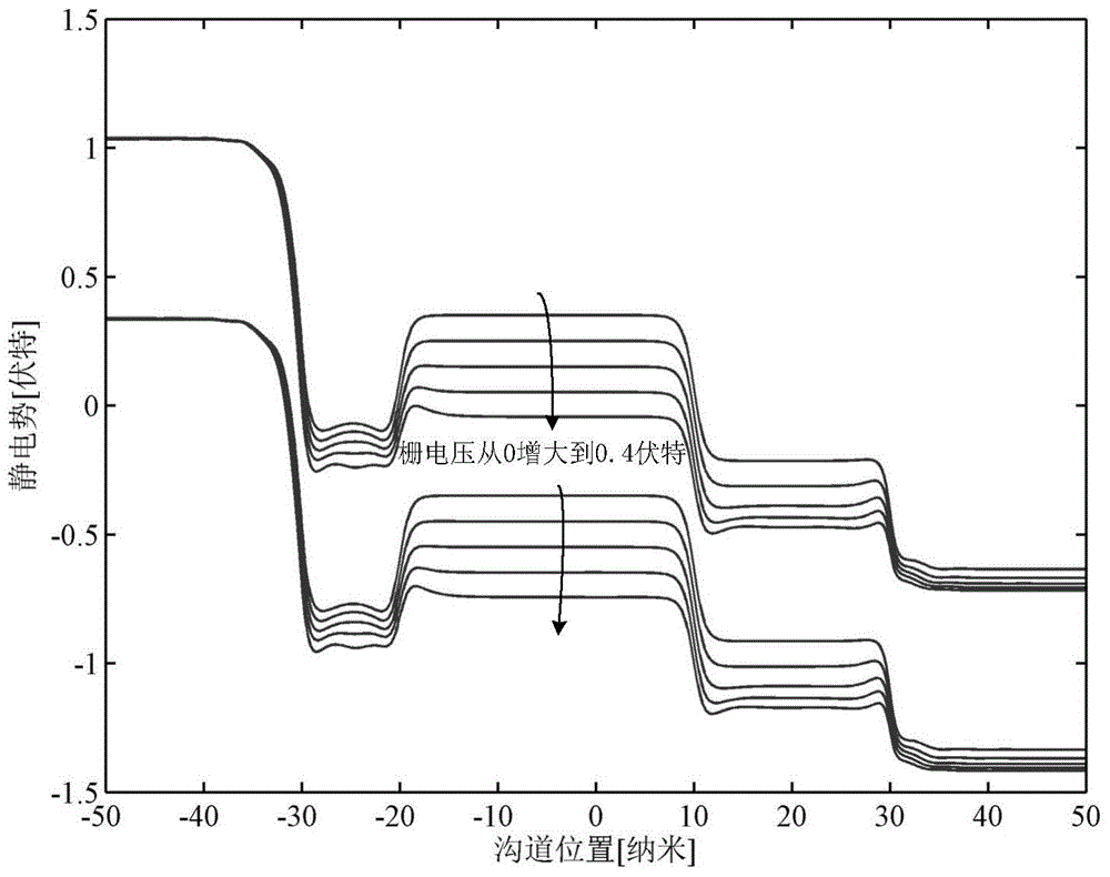
[0038] Such as figure 2 As shown, the different doping of the three ends in the channel region makes the potential in the channel segment 1, the channel segment 2 and the channel segment 3 have different energy band heights, and the channel segment 2 in the middle of the channel has a higher energy band A potential barrier is formed between channel segment 1 and channel segment 3; as the gate voltage increases from 0 volts to 0.4 volts, this potential barrier always exists, but the height changes with the gate voltage, which can be regulated by the gate It is used to regulate the tunneling current between source and drain.

Embodiment 2

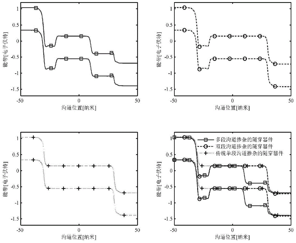
[0039] Embodiment 2: The channel length is 60 nanometers, the source and drain lengths are each 20 nanometers, the multi-segment channel-doped tunneling field effect device and the corresponding single-segment channel doping and double-segment channel doping tunneling field The influence of effect transistor devices on the energy band of the channel region.

[0040] Such as image 3 The band structure in , and Figure 4 As shown in the transfer characteristic curve in , compared with the traditional single-segment channel doped device, the doping in channel segment one increases the slope of the source-channel junction and increases the source-channel load. Carrier tunneling, thus increasing the on-state current of the device; on the other hand, compared with the two-segment channel doped device, the doping in the second channel segment makes the slope of the channel-drain junction decrease, reducing The carrier tunneling between the channel and the drain is suppressed, and ...

Embodiment 3

[0041] Embodiment 3: The channel length is 60 nanometers, the source and drain lengths are 20 nanometers each, and the effect of changing the doping concentration of channel segment 1 on the energy band structure.

[0042] Such as Figure 5 As shown, with the increase of the doping concentration of the channel segment 1, the change of the doping concentration between the source and the channel segment 2 is intensified, and the corresponding energy band bending of the channel segment 1 is increased.


PUM


Abstract

The invention belongs to the field of semiconductor integrated circuits, and specifically relates to a tunneling field effect device for channel potential barrier height control. The center of the device is provided with a channel, two ends of the channel are provided with a source terminal and a drain terminal of different conductive types, a tunneling junction is formed between the source terminal and the channel, the channel is formed by the adoption of three or more than three potential barrier areas, the energy band of the potential barrier area at the middle section is higher than the energy bands of the channel close to the drain terminal and the source terminal, the device also comprises a gate oxide layer fully covering the channel, and the gate oxide layer is fully covered by a gate electrode. The portion of the channel of the device employs materials of different doping concentrations or types, and three sections or more sections of the potential barrier structures are formed in the channel. According to the simulation research result of the tunneling device structure for channel potential barrier height control, the off-state leakage current of the device can be effectively reduced, the sub-threshold slope is reduced, the short-channel effect and the DIBL effect are suppressed, the transconductance characteristic is good, and comprehensive optimization of the performance of the device is realized.

Description

technical field [0001] The invention belongs to the field of semiconductor integrated circuits, and in particular relates to a tunneling field effect device with channel potential barrier height control. Background technique [0002] Tunneling field effect transistors are based on the tunneling transport between energy bands of carriers, and adopt a different working mechanism from the structure of traditional metal oxide semiconductor field effect devices. They have excellent sub-threshold characteristics and can be lower than traditional The physical limit of MOS FETs is 60 mV / dec, with very low leakage current. However, since the tunneling field effect transistor is based on the quantum tunneling of carriers between energy bands to realize carrier transport, its on-state current is relatively small and its driving ability is weak. On the other hand, except for the carrier at the source end Energy band transport can be realized, and the carriers at the drain can also be t...

Claims


Application Information

Patent Timeline
Patent Type & Authority Applications(China)
IPC IPC(8): H01L29/78H01L29/06H01L29/10
CPCH01L29/78H01L29/06H01L29/1041
Inventor 王豪常胜何进黄启俊
Owner WUHAN UNIV
Why Eureka
Try Eureka