III-V family nitride semiconductor epitaxial structure, device comprising epitaxial structure and preparation method thereof

A nitride semiconductor, III-V technology, used in semiconductor devices, electrical components, circuits, etc., can solve the problems of affecting device consistency, small process window, and high production costs

Inactive Publication Date: 2015-09-23
SHANGHAI XINYUANJI SEMICON TECH
View PDF4 Cites 6 Cited by
  • Summary
  • Abstract
  • Description
  • Claims
  • Application Information

AI Technical Summary

Problems solved by technology

The high-quality GaN epitaxial layer has a single crystal structure, and the production cost is high
Moreover, the thickness of GaN greater than 1 micron between the dielectric pattern and the sapphire surface will affect the effect of diffuse scattering, and GaN greater than 1 micron will also a

Method used


Image

  • III-V family nitride semiconductor epitaxial structure, device comprising epitaxial structure and preparation method thereof
  • III-V family nitride semiconductor epitaxial structure, device comprising epitaxial structure and preparation method thereof
  • III-V family nitride semiconductor epitaxial structure, device comprising epitaxial structure and preparation method thereof

Examples


Embodiment 1

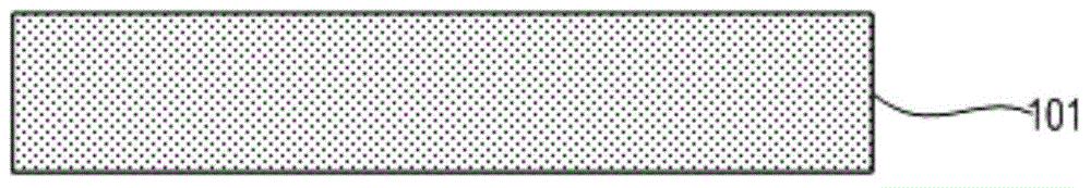
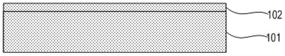
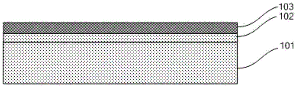
[0130] Such as Figure 1 - Figure 1 As shown in 1, this embodiment provides a III-V group nitride device structure including a microscopic cavity structure and a manufacturing method thereof, comprising the following steps:

[0131] 1. If figure 1 As shown, in this embodiment, the growth substrate 101 is a commercially available flat Al 2 o 3 The substrate, whose surface crystal orientation (0001), has atomic-level flatness. In this embodiment, a no-clean substrate is used, which can be used directly without cleaning. Place the above substrate on a graphite tray with a SiC protective layer and send it into a metal organic chemical vapor deposition (MOCVD) reaction chamber; heat the above substrate to 1100°C under a hydrogen atmosphere and keep it at this temperature for 10 minutes ; Then the substrate temperature is reduced to 550°C, and ammonia gas, trimethylaluminum (TMAl) and trimethylgallium (TMGa) are simultaneously fed into the reaction chamber, wherein the standard...

Embodiment 2

[0153] Such as Figure 1 - Figure 1 As shown in 1, the III-V group nitride device including the microscopic cavity structure provided by this embodiment, its basic steps are as in embodiment 1, the only difference is the third step: patterning the semiconductor dielectric layer 103 as periodic Sexually spaced SiO 2 Lines with a width of 7 μm at the bottom of the line and a spacing of 3 μm.

[0154] The luminous flux of the packaged 14mil*28mil LED chip prepared in this embodiment is 20.21lm, and its ESD human body model 4000V passing rate is 93% on average.


PUM

PropertyMeasurementUnit
Thicknessaaaaaaaaaa

Abstract

The invention relates to a III-V family nitride semiconductor epitaxial structure comprising a (1) substrate; (2) an epitaxial buffer layer; (3) an epitaxial transition layer; and (4) an epitaxial effective layer. The epitaxial buffer layer is provided with an upper surface and a lower surface which is contacted with the substrate. The epitaxial transition layer covers the epitaxial buffer layer, and a microscopic hole structure is arranged at the interface of the epitaxial transition layer and the epitaxial buffer layer. The microscopic holes are periodically or non-periodically arranged so that the interface of the epitaxial transition layer and the epitaxial buffer layer is enabled to be partially connected, and the connected parts and the hole parts appear in a spacing way at the interface. The epitaxial transition layer is provided with a flat upper surface. The epitaxial effective layer is arranged at the upper surface of the epitaxial transition layer. The epitaxial effective layer comprises an n-type epitaxial layer, a luminescent layer and a p-type epitaxial layer which are arranged from the bottom to the top. The invention also provides a manufacturing method of the epitaxial structure, a device comprising the epitaxial structure and a manufacturing method thereof.

Description

technical field [0001] The present invention relates to the field of semiconductor lighting, and more specifically relates to a III-V nitride semiconductor epitaxial wafer, a device including the epitaxial wafer and a manufacturing method thereof. Background technique [0002] As a new type of high-efficiency solid-state light source, semiconductor lighting has the advantages of long life, energy saving, environmental protection, safety, etc., and its application field is expanding rapidly. The core of semiconductor lighting is a light-emitting diode (LED). From a structural point of view, an LED is composed of III-V compounds, such as GaAs (gallium arsenide), GaP (gallium phosphide), GaAsP (gallium arsenide phosphide), GaN (nitrogen PN junction formed by semiconductors such as gallium chloride). Therefore, it has the I-V characteristics of a general PN junction, that is, forward conduction, reverse cutoff, and breakdown characteristics. In addition, under certain conditio...

Claims


Application Information

Patent Timeline
IPC IPC(8): H01L33/32H01L33/16
CPCH01L33/32H01L33/0075H01L33/16
Inventor 郝茂盛袁根如
Owner SHANGHAI XINYUANJI SEMICON TECH
Why Eureka
Try Eureka