Laser resistance welding power module

A technology of power modules and solder resistance, which is applied in the direction of electrical components, electric solid devices, circuits, etc., can solve the problems of reduced flexibility, loss of solder resistance, and falling off, etc., and achieves the effect of reliable method, strong flexibility and simple structure

Active Publication Date: 2015-09-30
STARPOWER SEMICON
View PDF3 Cites 3 Cited by
  • Summary
  • Abstract
  • Description
  • Claims
  • Application Information

AI Technical Summary

Problems solved by technology

[0004] The method of adding solder mask or solder mask wire requires an additional process cost and the cost of solder mask material and stencil, and it takes time and temperature to cure the solder mask layer or solder mask wire
On the other hand, in the process of forming the solder resist layer or solder resist line, certain pollution will be generated on the soldering surface
In addition, the solder resist layer or solder resist wire tends to fall off during the soldering heating process, thus losing the function of solder resist
[0005] There is no cost problem in adding full-through or half-through positioning holes, but after adding holes, the conductivity of the welding surface as a metal conductor will be affected
In addition, after the positioning holes are formed, the area that can be welded will be reduced accordingly, and the types of components to be welded will be limited due to the size problem, and the flexibility will be reduced.

Method used


Image

  • Laser resistance welding power module
  • Laser resistance welding power module
  • Laser resistance welding power module

Examples


Embodiment

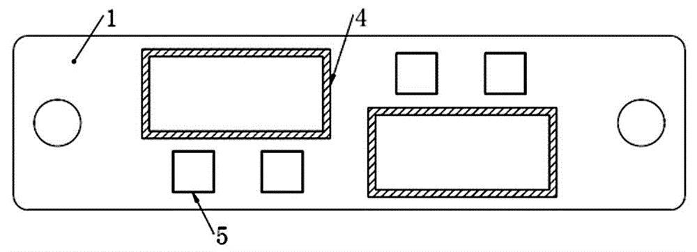
[0020] figure 1 According to the layout design of the power module, it is a style of laser soldering on the copper substrate 1 . The solder resist patterns 4 and 5 formed by laser etching on the copper substrate 1 include a rectangular wire frame 4 with a wire diameter of 1 mm for DBC soldering and a rectangular wire frame 5 with a wire diameter of 0.1 mm for chip soldering.

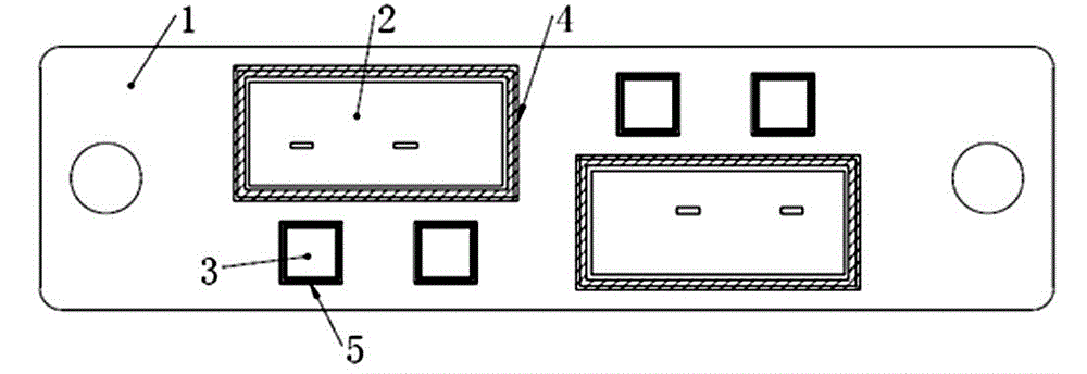
[0021] figure 2 It is a semi-finished power module with a chip 3 and a copper-clad ceramic substrate (DBC) 2 mounted thereon.

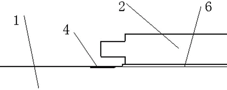
[0022] according to image 3 As shown, the minimum distance between the solder 6 and one side of the solder resist area 4 is about 0.3 mm, and the minimum distance between the edge of the lower copper layer of the copper-clad ceramic substrate (DBC) 2 and the solder resist area 4 is about 0.4 mm.

[0023] according to Figure 4 As shown, the minimum single-side distance between the solder 7 and the solder resist area 5 is about 0.1 mm, and the minimum single-side distance b...


PUM


Abstract

A laser beam resistance welding power module mainly comprises a semiconductor chip, a copper clad ceramic substrate, welding flux and a copper substrate. Resistance welding graphic wire frames for welding the copper clad ceramic substrate and the semiconductor chip respectively are etched on the copper substrate by laser beams, the semiconductor chip and the copper clad ceramic substrate are respectively welded in the resistance welding graphic wire frames on the copper substrate through the welding flux, the wire diameter of the resistance welding graphic wire frame for welding the copper clad ceramic substrate is 1mm, the wire diameter of the resistance welding graphic wire frame for welding the semiconductor chip is 0.1mm, the minimum unilateral distance between the welding flux and an area of the corresponding resistance welding graphic wire frame is 0.3mm, the minimum unilateral distance between the edge of a lower copper layer of the copper clad ceramic substrate and an area of the corresponding resistance welding graphic wire frame is 0.4mm, the power of the laser beams is controlled within a certain range, and the surface of the copper substrate treated by the laser beams can stop the welding flux and elements from position movement at a melting stage in the welding process.

Description

technical field [0001] The invention relates to a power module using laser welding resistance, which belongs to the field of semiconductor module packaging. Background technique [0002] The soldering process is affected by the wettability of the solder itself, the unevenness of the solder sheet, the volatilization and flow of the flux, the movement of the pores generated during the soldering process, the pollution or inequality of the soldering surface, often resulting in the occurrence or failure of the required soldering components. More or less location moves. This movement will cause difficulties in subsequent processes such as wire bonding, packaging of the housing, and the like. Therefore, in the packaging process of semiconductor power modules, it is necessary to try to avoid the positional movement of the soldered components during the soldering process. [0003] Traditional solder mask methods generally include printing solder mask materials to form solder mask l...

Claims


Application Information

Patent Timeline
Patent Type & Authority Applications(China)
IPC IPC(8): H01L23/492H01L21/48H01L21/60
CPCH01L21/4871H01L23/492H01L24/81H01L2224/81
Inventor 许林锋
Owner STARPOWER SEMICON
Why Eureka
Try Eureka