Diamond wire cutting-based silicon wafer texturing pretreatment method and silicon wafer texturing method

A diamond wire cutting and pretreatment technology, applied in post-processing, post-processing details, chemical instruments and methods, etc., can solve the problems that the reflectivity of silicon wafers cannot meet the requirements of industrial production, it is difficult to eliminate, and the application and promotion of diamond cutting technology is limited. , to achieve the effect of low cost, reduced surface reflectivity, and no trace

Inactive Publication Date: 2015-10-07
NINGBO INST OF MATERIALS TECH & ENG CHINESE ACADEMY OF SCI
View PDF5 Cites 18 Cited by
  • Summary
  • Abstract
  • Description
  • Claims
  • Application Information

AI Technical Summary

Problems solved by technology

[0003] However, there are a series of problems in the surface texturing of polycrystalline silicon wafers, which limit the application and promotion of diamond cutting technology
For example, diamond cutting technology is easy to form cutting lines on silicon wafers during cutting, but the cutting lines are difficult to eliminate when using conventional acid etching methods for texturing, that is, the surface of silicon wafers after texturing still has cutting lines, so that The reflectivity of the silicon wafer after texturing cannot meet the requirements of industrial production, etc.

Method used


Image

  • Diamond wire cutting-based silicon wafer texturing pretreatment method and silicon wafer texturing method
  • Diamond wire cutting-based silicon wafer texturing pretreatment method and silicon wafer texturing method
  • Diamond wire cutting-based silicon wafer texturing pretreatment method and silicon wafer texturing method

Examples


Embodiment 1

[0061] Mix 40wt% hydrofluoric acid solution, 30wt% hydrogen peroxide solution and water at a volume ratio of 3:24:5, and add silver nitrate to obtain a pretreatment solution. The silver nitrate concentration in the pretreatment liquid is 80 μmol / L.

[0062] Use 10wt% hydrofluoric acid solution to remove oil stains and oxide layers on the silicon wafer surface cut by diamond wire, then place the silicon wafer in the pretreatment solution to carry out pretreatment A process, the pretreatment temperature is 25 ° C, and the pretreatment time is 5 minutes. Then rinse with deionized water for 2 minutes, soak in nitric acid for 2 minutes to remove silver particles on the surface, and rinse with deionized water for 2 minutes.

[0063] Repeat the pretreatment B process by putting the above silicon wafers into the pretreatment solution, the pretreatment temperature is 25° C., and the pretreatment time is 1 minute. Then rinse with deionized water for 2 minutes.

[0064] Mix 40wt% hydr...

Embodiment 2

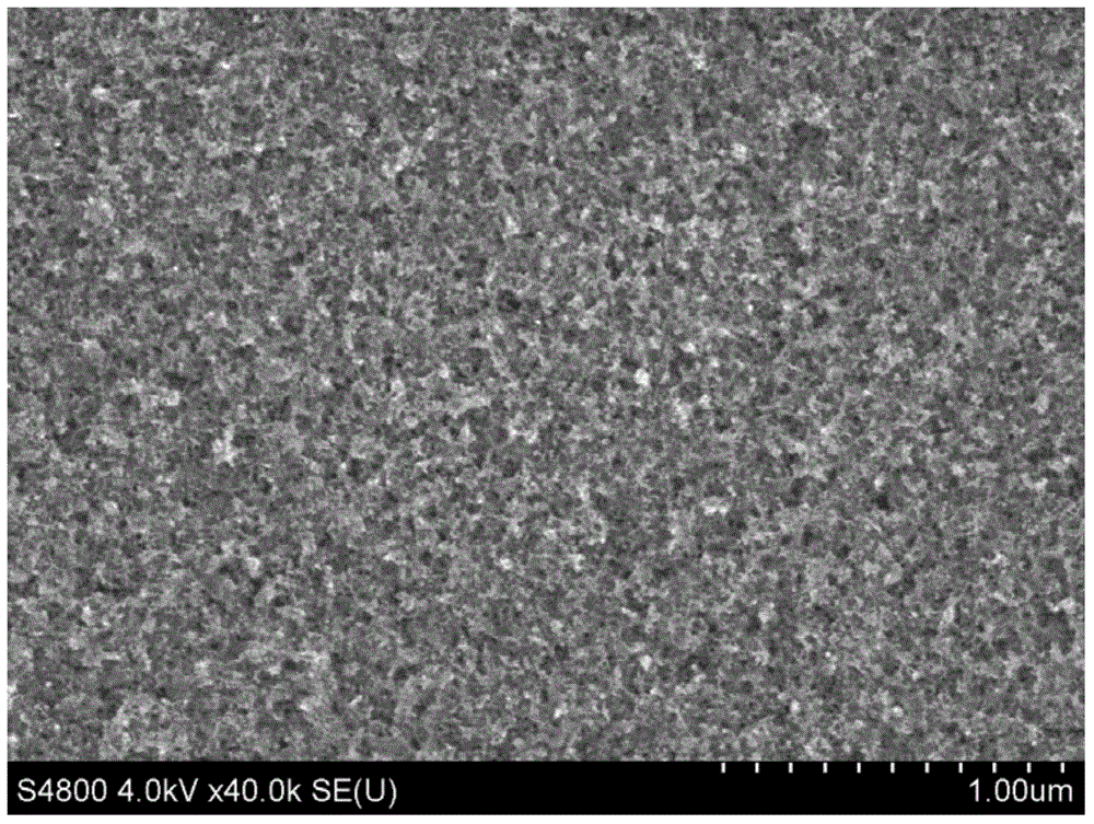
[0066] The velvet pretreatment method and the velvet method of embodiment 2 are basically the same as the velvet pretreatment method and the velvet method of embodiment 1, the difference is that the pretreatment liquid is composed of 40wt% hydrofluoric acid solution and 30wt% hydrogen peroxide The solution was mixed at a volume ratio of 5:18, the concentration of silver nitrate in the pretreatment solution was 3 μmol / L, the pretreatment A process time was 10 minutes, and the pretreatment B process reaction time was 3 minutes. Figure 4 It is the SEM image of the surface after silicon wafer pretreatment, Figure 5 SEM image of the surface of the silicon wafer after texturing.

Embodiment 3

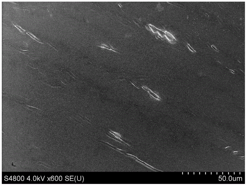
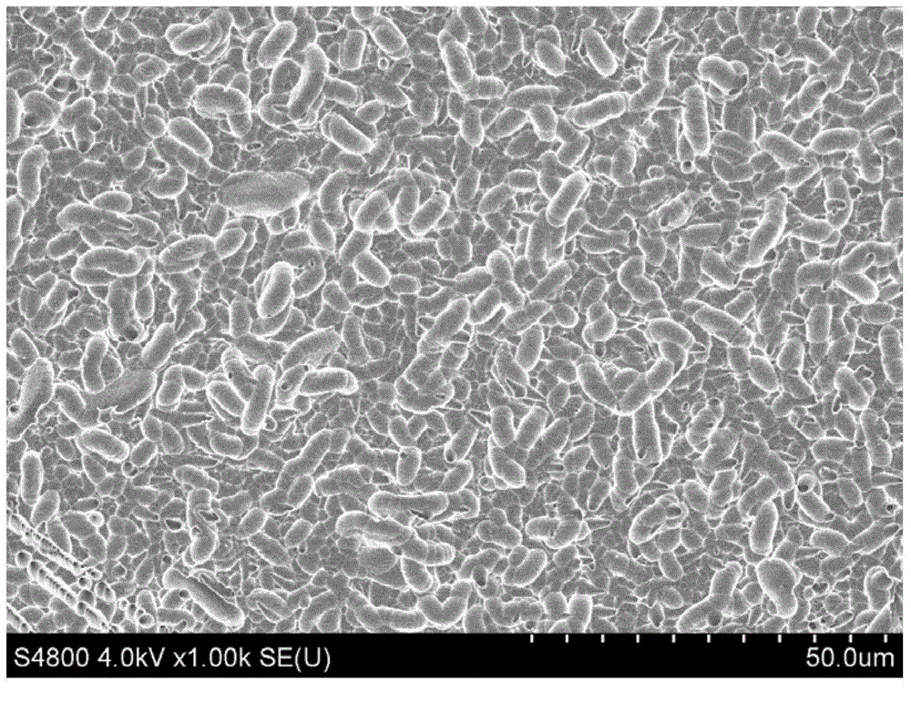
[0068] The texturing pretreatment method and texturing method of embodiment 3 are basically the same as the texturing pretreatment method and texturing method of embodiment 1, the difference lies in the pretreatment liquid concentration and pretreatment B process time, 50wt% hydrofluoric acid Solution, 30wt% hydrogen peroxide solution and 89% isopropanol are mixed with a volume ratio of 1:20:3, the metal salt in the pretreatment solution is copper nitrate, and the concentration of the copper nitrate solution is 1000 μmol / L, pretreatment A The process time is 9 minutes, and the pretreatment temperature is 40°C; the reaction time of the pretreatment B process is 40 seconds, and the treatment temperature is 30°C. Pretreatment A process reaction time and temperature are identical with embodiment 1. Figure 6 It is the SEM image of the surface after silicon wafer pretreatment, Figure 7 SEM image of the surface of the silicon wafer after texturing.


PUM


Abstract

The invention provides a diamond wire cutting-based silicon wafer texturing pretreatment method. The method comprises the following steps: a, mixing a hydrofluoric acid solution, a hydrogen dioxide solution, metal salt and water to obtain pretreatment liquid; b, putting a silicon wafer cut by a diamond wire into the pretreatment liquid and performing pretreatment A, until cutting lines on the silicon wafer are basically removed; c, cleaning the silicon wafer subjected to pretreatment A by an acid solution, so as to remove metal particles on the silicon wafer; d, putting the silicon wafer cleaned by the acid solution into the pretreatment liquid and performing pretreatment B, and forming a pretreatment texturing surface with a uniform micro / nano structure on the silicon wafer. The invention also provides a diamond wire cutting-based silicon wafer texturing method.

Description

technical field [0001] The invention relates to the field of texturing of crystalline silicon solar cells, in particular to the technical field of texturing of silicon wafers based on diamond wire cutting. Background technique [0002] Diamond wire cutting technology, also known as fixed abrasive diamond wire sawing, is usually made by fixing diamond particles in the nickel-based alloy layer on the surface of stainless steel wire by electroplating or resin fixing. During the cutting process, the diamond wire saw runs at high speed and directly grinds and cuts the silicon material with a certain pressure. Compared with the traditional mortar multi-wire cutting technology, the diamond wire cutting technology has the advantages of high cutting efficiency, low cutting processing cost and clean environment, and is expected to become the future development direction of cutting hard and brittle materials such as crystalline silicon in the photovoltaic field. [0003] However, ther...

Claims


Application Information

Patent Timeline
Patent Type & Authority Applications(China)
IPC IPC(8): C30B33/10H01L31/18
CPCY02P70/50
Inventor 应智琴叶继春高平奇韩灿廖明墩
Owner NINGBO INST OF MATERIALS TECH & ENG CHINESE ACADEMY OF SCI
Why Eureka
Try Eureka