
Manufacturing method of crystalline silicon solar cell

A technology of solar cells and manufacturing methods, applied in the field of solar cells, capable of solving problems such as high series resistance and low open circuit voltage

Inactive Publication Date: 2015-10-07
SICHUAN YINHE STARSOURCE TECH CO LTD
View PDF7 Cites 19 Cited by
  • Summary
  • Abstract
  • Description
  • Claims
  • Application Information

AI Technical Summary

Problems solved by technology

However, these passivation films are insulators, which block the electrical contact of the metal on the silicon, although the current fire-through silver can burn through SiN better. x Form a better electrical contact and form a gate electrode on the front of the solar cell, but the actual gate electrode contact resistivity is often greater than 1mΩ.cm 2 , resulting in low open circuit voltage (Voc) and high series resistance, and requires a high sintering temperature to burn through the passivation film

Method used

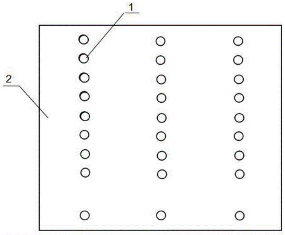
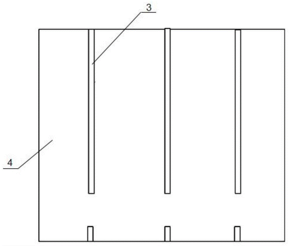
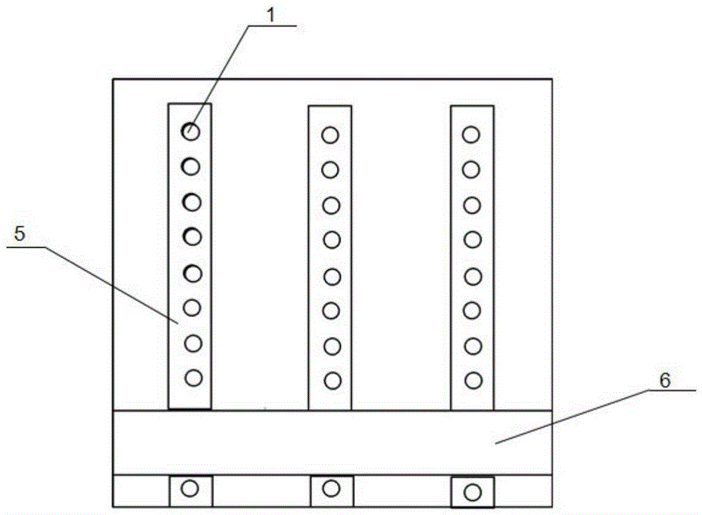

Image

  • Manufacturing method of crystalline silicon solar cell
  • Manufacturing method of crystalline silicon solar cell
  • Manufacturing method of crystalline silicon solar cell

Examples


Embodiment 1

[0047] The manufacturing method of n-type double-sided solar cells: Take an n-type single crystal silicon, use 15-30% alkali solution to perform corrosion cleaning on the single crystal silicon at 80-100°C for 0.5-1min, to remove oil stains, cut Damaged layer, etc., the cleaned single crystal silicon is formed on the surface of the silicon wafer by mechanical grooving, chemical etching, reactive ion etching, laser grooving and other methods to reduce surface reflection loss, and then use diffusion The p-diffusion layer is formed on the front side of the silicon wafer to form a PN junction; then, the n-diffusion layer is formed on the back side by a diffusion method to form an n + Floor. For example, by using atmospheric pressure chemical vapor deposition (APCVD), borosilicate glass (BSG) is deposited at 500-800°C for boron diffusion and deposition of SiO 2 membrane, then with POCl 3 Phosphorus diffusion is carried out by liquid source diffusion method, that is, through a cer...

Embodiment 2

[0054] Passivated Emitter Rear Contact (PERC) silicon solar cells increase the conversion efficiency of the cell by adding a qualitative passivation layer on the back of the cell. This technique prepares SiO on the back surface of conventional cells. 2 、Al 2 o 3 , SiOx or Al 2 o 3 / SiN x The passivation film maximizes the potential difference between the p-n junctions and reduces the recombination of electrons, thereby improving battery efficiency. PECR batteries require laser etching on the back passivation layer, and then make the aluminum paste locally form a back electric field battery (BSF ) and electrical contacts, thereby increasing Voc and Isc. In this method, the front side of the battery is also partially etched at the same time, and a local electric contact is formed on the etched silicon surface with a non-burn-through silver paste. The sintering temperature of the battery can be greatly reduced by using the non-fire-through paste, and the sintering peak tempe...


PUM

PropertyMeasurementUnit
diameteraaaaaaaaaa
widthaaaaaaaaaa
thicknessaaaaaaaaaa

Abstract

The invention discloses a manufacturing method of a crystalline silicon solar cell. The manufacturing method includes the following steps that: surface treatment is performed on a cleaned silicon wafer, so that a concavo-convex texturized surface can be obtained; a PN junction is formed on the silicon wafer through adopting a diffusion method; the silicon wafer periphery of the formed PN junction is etched, so that a redundant diffusion layer can be removed, and a film body is deposited on the front surface and the back surface of the silicon wafer respectively, and local film body portions are removed through adopting an etching method, so that dot-shaped or stripe-shaped structures which uniformly expose the silicon wafer can be formed on the film bodies; a front surface conductive paste and a back surface conductive paste are printed on the front surface and the back surface of the silicon wafer respectively; and sintering is performed, so that the solar cell can be obtained. According to the manufacturing method of the invention, the etching method is adopted for the film bodies on the solar cell, so that the local film body portions are removed through etching, and the non-burn-through conductive pastes are printed on the locally-etched film bodies, and therefore, direct electric contact between local metal and silicon can be realized, and the film bodies will not be damaged in high-temperature sintering of the conductive pastes as much as possible, and the open-circuit voltage of the solar cell can be increased, and the contact resistance of the solar cell can be reduced, and therefore, the conversion efficiency of the solar cell can be improved.

Description

technical field [0001] The invention belongs to the technical field of solar cells, in particular to a method for manufacturing a partially electrically contacted crystalline silicon solar cell. Background technique [0002] In recent years, the annual growth rate of photovoltaic cell production is very fast. Solar photovoltaic power generation will occupy an important seat in the world's energy consumption in the near future. It will not only replace some conventional energy sources, but also become the main body of the world's energy supply. At present, crystalline silicon cells are the main body of photovoltaic cells. Although the share of crystalline silicon solar cells will decline due to the development of thin-film solar cells or other new types of cells in the next 10 years, its dominant position will not change fundamentally. [0003] Current crystalline silicon solar cells are fabricated from n-type or p-type silicon. N-type silicon wafers usually have a longer ca...

Claims


Application Information

Patent Timeline
Patent Type & Authority Applications(China)
IPC IPC(8): H01L31/18
CPCH01L31/1804Y02E10/547Y02P70/50
Inventor 李运钧尹天平曾国平杨墨熹李昕
Owner SICHUAN YINHE STARSOURCE TECH CO LTD
Learn More