
Method for improving channel mobility of SiC metal-oxide-semiconductor field-effect transistor (MOSFET)

A mobility and channel technology, applied in the field of microelectronics, can solve the problems of device channel mobility and on-resistance degradation, device performance not reaching device performance, restricting the development of SiC power devices, etc., to improve channel migration. rate, improve performance

Active Publication Date: 2015-11-11
瑶芯微电子科技(上海)有限公司
View PDF4 Cites 11 Cited by
  • Summary
  • Abstract
  • Description
  • Claims
  • Application Information

AI Technical Summary

Problems solved by technology

[0003] However, at present, the main material of the gate dielectric of SiC power MOS devices is SiO2 generated by thermal oxidation, but the quality of the contact interface between SiC and SiO2 is poor, and the high density of interface states and interface roughness lead to serious degradation of device channel mobility and on-resistance , even making the performance of SiC-based devices fall short of those of Si-based devices
Although the interface state can be partially reduced by introducing nitride components during the annealing process through process improvement, the problem of C atom complexes at the interface between SiC and SiO2 during the oxidation process cannot be fundamentally solved, which also makes the channel of SiC The mobility has been very low, seriously restricting the development of SiC power devices

Method used


Image

  • Method for improving channel mobility of SiC metal-oxide-semiconductor field-effect transistor (MOSFET)
  • Method for improving channel mobility of SiC metal-oxide-semiconductor field-effect transistor (MOSFET)
  • Method for improving channel mobility of SiC metal-oxide-semiconductor field-effect transistor (MOSFET)

Examples


Embodiment Construction

[0042] The technical solutions of the present invention will be described in further detail below with reference to the accompanying drawings and embodiments.

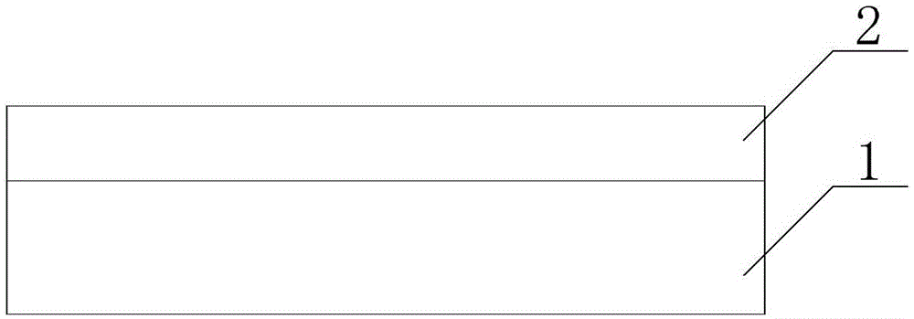
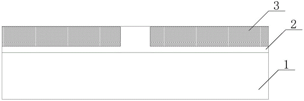
[0043] First of all, it should be explained that the method for improving the channel mobility of SiCMOSFET power devices provided by the embodiments of the present invention can be used in the manufacturing process of SiCMOSFETs with various conductive structures, specifically including but not limited to: laterally diffused metal oxide semiconductor Field effect transistor (LaterallyDiffusedMOSFET, LDMOSFET), vertical double-diffused metal oxide semiconductor field effect transistor (verticaldouble-diffusedMOSFET, VDMOSFET), vertical channel V-groove metal oxide semiconductor (vertical-channelV-grooveMOSFET, VVMOSFET), U-shaped groove Metal Oxide Semiconductor (U-shapedgroove MOSFET, UMOSFET), etc. Although VDMOSFET is used as an example for illustration in the following schematic diagram of the specific process of t...


PUM


Abstract

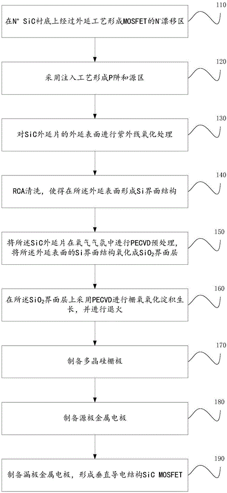
The embodiment of the invention relates to a method for improving the channel mobility of a SiC metal-oxide-semiconductor field-effect transistor (MOSFET). The method comprises the following steps: before gate-oxide is carried out, carrying out ultraviolet oxidation treatment on the epitaxy surface of SiC epitaxial wafer; carrying out rubisco activase (RCA) cleaning, and forming an Si interface structure on the epitaxy surface; carrying out plasma enhanced chemical vapor deposition (PECVD) pretreatment on the SiC epitaxial wafer in oxygen atmosphere, and oxidizing the Si interface structure of the epitaxy surface into an SiO2 interface layer; carrying out gate-oxide oxidizing deposition growth on the SiO2 interface layer by PECVD, and carrying out annealing; and preparing a polycrystalline silicon gate and source and drain metal electrodes, so as to form the SiC MOSFET.

Description

technical field [0001] The invention relates to the technical field of microelectronics, in particular to a method for improving SiC MOSFET channel mobility. Background technique [0002] SiC has become one of the most advantageous semiconductor materials for manufacturing high-temperature, high-power electronic devices due to its excellent physical, chemical and electrical properties, and has a power device quality factor much greater than that of Si materials. The research and development of SiC power device Metal-Oxide-Semiconductor Field-Effect Transistor (Metal-Oxide-Semiconductor Field-Effect Transistor, MOSFET) began in the 1990s. It has high input impedance, fast switching speed, high operating frequency, and high temperature and high pressure resistance. The advantages of the series have been widely used in switching regulated power supplies, high-frequency heating, automotive electronics, and power amplifiers. [0003] However, at present, the main material of the...

Claims


Application Information

Patent Timeline
IPC IPC(8): H01L21/02H01L21/336H01L29/12
CPCH01L21/02057H01L29/1608H01L29/66712
Inventor 贾仁需汪钰成吕红亮张玉明
Owner 瑶芯微电子科技(上海)有限公司
Learn More