MEMS pressure sensor and preparation method thereof

A pressure sensor and pressure technology, used in fluid pressure measurement using capacitance change, piezoelectric/electrostrictive/magnetostrictive devices, instruments, etc., can solve problems such as poor contact of interconnect structures, and improve performance and yield. , the effect of good adjustment effect

Active Publication Date: 2015-11-25
SEMICON MFG INT (SHANGHAI) CORP
View PDF5 Cites 11 Cited by
  • Summary
  • Abstract
  • Description
  • Claims
  • Application Information

AI Technical Summary

Problems solved by technology

[0009] at 0.6J / cm 2 Under the action of laser annealing, the temperature of the adhesive layer 105 (gluelayer) between SiGe and Al is as high as 900°C, which will cause Al melting (melting), resulting in the opening of the interconnection structure, and the interconnection structure is in poor contact. The problem

Method used


Image

  • MEMS pressure sensor and preparation method thereof
  • MEMS pressure sensor and preparation method thereof
  • MEMS pressure sensor and preparation method thereof

Examples


Embodiment 1

[0069] Attached below figure 2 And attached Figure 3a-3b The pressure sensor of the present invention will be further described.

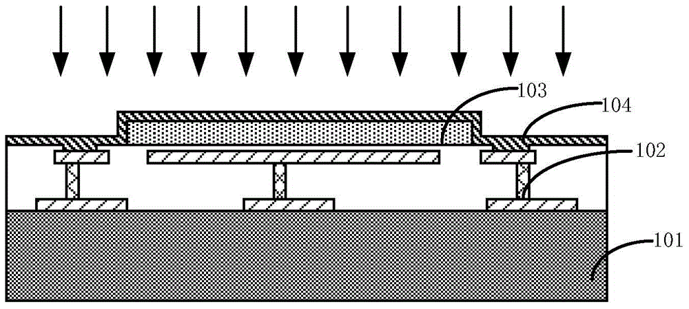
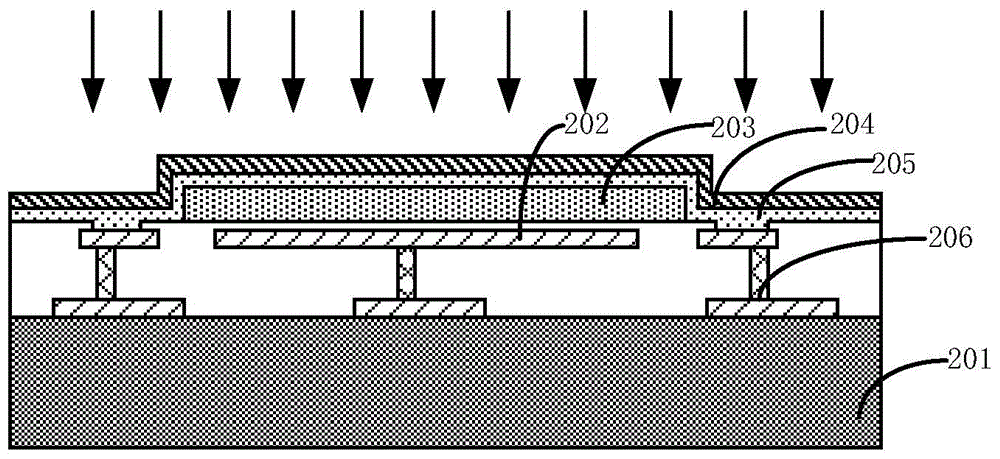
[0070] Such as figure 2 As shown, the pressure sensor includes:

[0071] A substrate 201, wherein a CMOS device is formed in the substrate 201;

[0072] a bottom electrode 202, located above the substrate 201;

[0073] a pressure sensor cavity, located above the bottom electrode 202;

[0074] A thermal isolation layer 205, surrounding the cavity of the pressure sensor, covering the substrate 201;

[0075] The pressure sensing film 204 is located above the heat isolation layer 205 .

[0076] Wherein, the pressure sensor includes a sensing area at the center and metal interconnection areas at both sides of the sensing area.

[0077] Wherein, a CMOS device is formed in the base 201, preferably, the base 201 includes at least a semiconductor substrate, and active devices and / or passive devices are formed in the semiconductor substrate, wherei...

Embodiment 2

[0106] The present invention also provides a method for preparing the pressure sensor, specifically comprising the following steps:

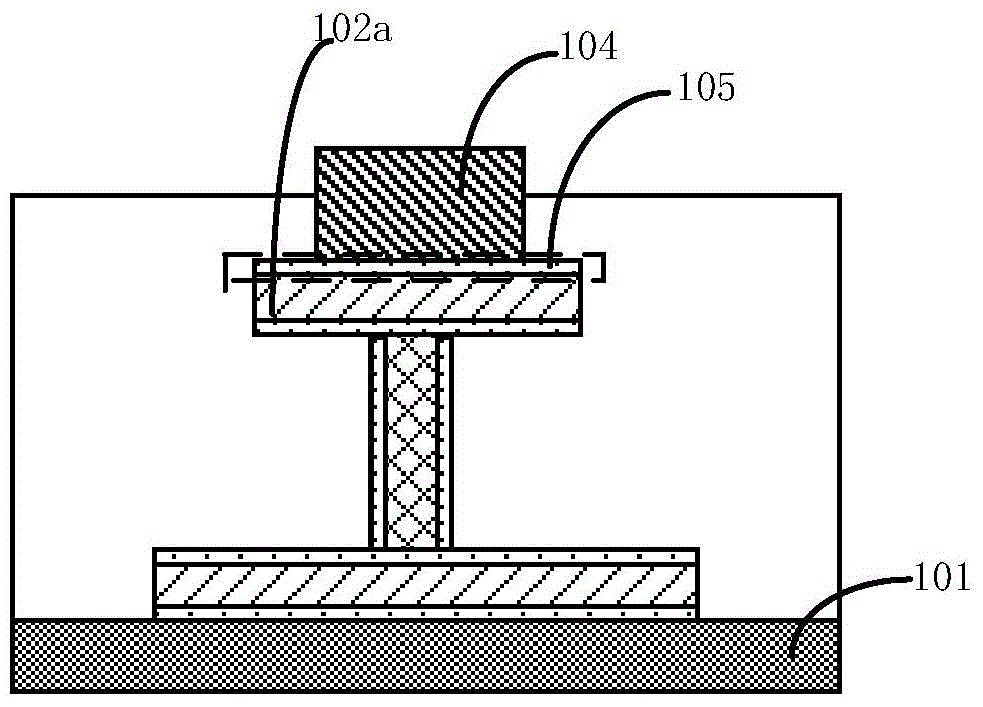
[0107] Step 201 is performed to provide a substrate 201 on which a bottom electrode 202 is formed, and a top electrode interconnection structure is formed on both sides of the bottom electrode 202 .

[0108] Specifically, in this step, the base 201 includes at least a semiconductor substrate, and active devices and / or passive devices are formed in the semiconductor substrate, wherein the types and numbers of the active devices and passive devices Can be selected according to specific needs, not limited to a certain one.

[0109] As preferably, an interlayer dielectric layer is formed on the semiconductor substrate, and SiO is selected in a specific embodiment of the present invention. 2 , but not limited to this instance.

[0110] Patterning the interlayer dielectric layer to form an Al metal layer in the interlayer dielectric layer as the bot...


PUM

PropertyMeasurementUnit
melting pointaaaaaaaaaa
thermal conductivityaaaaaaaaaa
thicknessaaaaaaaaaa

Abstract

The invention relates to an MEMS pressure sensor and a preparation method thereof. The preparation method comprises the steps of providing a substrate on which an interlayer dielectric layer and a bottom electrode in the interlayer dielectric layer are formed; forming a patterned sacrificial material layer above the bottom electrode; forming a thermal insulation layer above the sacrificial material layer and the interlayer dielectric layer for covering the sacrificial material layer and the interlayer dielectric layer; forming a pressure sensing film on the thermal insulation layer as a top electrode; and performing a laser annealing step for improving the stress performance of the pressure sensing film. The MEMS pressure sensor and the preparation method are advantageous in that (1) no thermal damage to the sacrificial material layer (amorphous carbon) is realized; (2) no thermal damage to a metal layer (Al) in the interconnecting structure of the top electrode is realized; (3) a good adjusting effect for the stress of the insulation layer poly-SiGe is obtained; and (4) breakage or failure of the interconnecting structure of the top electrode is prevented, thereby improving the performance and yield rate of the device.

Description

technical field [0001] The invention relates to the field of semiconductors, in particular, the invention relates to a MEMS pressure sensor and a preparation method thereof. Background technique [0002] With the continuous development of semiconductor technology, smart phones, integrated CMOS and micro-electromechanical systems (MEMS) devices have increasingly become the most mainstream and advanced technologies in the market for motion sensors (motion sensors), and with technology updates, The development direction of this kind of transmission sensor products is smaller size, high-quality electrical performance and lower loss. [0003] Among them, MEMS pressure sensors are widely used in automotive electronics: such as TPMS, engine oil pressure sensor, air pressure sensor of automobile brake system, automobile engine intake manifold pressure sensor (TMAP), diesel common rail pressure sensor; consumer electronics: such as tire pressure Meters, sphygmomanometers, cabinet sc...

Claims


Application Information

Patent Timeline
Patent Type & Authority Applications(China)
IPC IPC(8): G01L1/14G01L9/12B81B7/02B81C1/00
Inventor 张先明伏广才
Owner SEMICON MFG INT (SHANGHAI) CORP
Why Eureka
Try Eureka