HEMT device with junction type semiconductor layer

A semiconductor and junction technology, applied in the field of HEMT devices, can solve problems such as limiting gate voltage swing, and achieve the effects of increasing off-state breakdown voltage, improving electric field concentration effect, and uniform electric field distribution

Active Publication Date: 2015-11-25
UNIV OF ELECTRONICS SCI & TECH OF CHINA
View PDF2 Cites 14 Cited by
  • Summary
  • Abstract
  • Description
  • Claims
  • Application Information

AI Technical Summary

Problems solved by technology

However, the top layer of GaN and the gate electrode form an ohmic contact of holes. When the gate is conducting forward, the gate leakage current will be generated when the gate voltage is large, which limits the gate voltage swing.

Method used


Image

  • HEMT device with junction type semiconductor layer
  • HEMT device with junction type semiconductor layer
  • HEMT device with junction type semiconductor layer

Examples


Embodiment 1

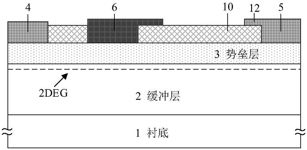
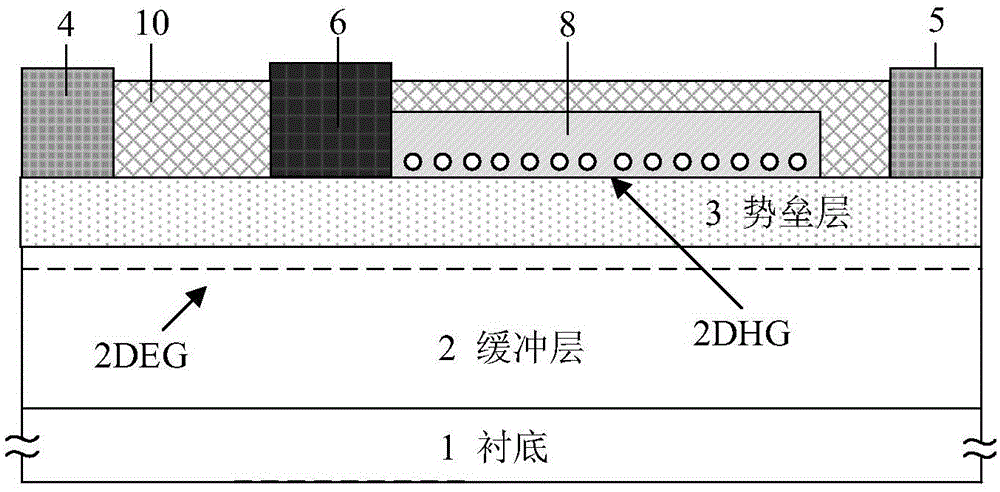
[0034] Such as Figure 4As shown, this example includes a substrate 1, a buffer layer 2 disposed on the upper surface of the substrate 1, and a barrier layer 3 disposed on the upper surface of the buffer layer 2, and the contact surface of the buffer layer 2 and the barrier layer 3 forms a The first heterojunction of a two-dimensional electron gas channel (2DEG); the two ends of the upper surface of the barrier layer 3 respectively have a source electrode 4 and a drain electrode 5, and the middle part of the upper surface of the barrier layer 3 has a gate structure; The upper surface of the barrier layer 3 between the source electrode 4 and the gate structure has a dielectric passivation layer 10, and the upper surface of the barrier layer 3 between the drain electrode 5 and the gate structure has a junction semiconductor layer 8; The contact surface between the junction semiconductor layer 8 and the barrier layer 3 forms a second heterojunction with two-dimensional hole gas (...

Embodiment 2

[0037] Such as Figure 5 As shown, the difference between this example and Example 1 is that the device rectification structure 9 of this example is a PN junction rectifier, and other structures are the same as those of Example 1. The rectifier structure and the P-type region of the junction semiconductor layer form a PN junction, which prevents the leakage current of the gate-2DHG-2DEG from being caused by a positive voltage on the gate, resulting in premature breakdown of the device.

Embodiment 3

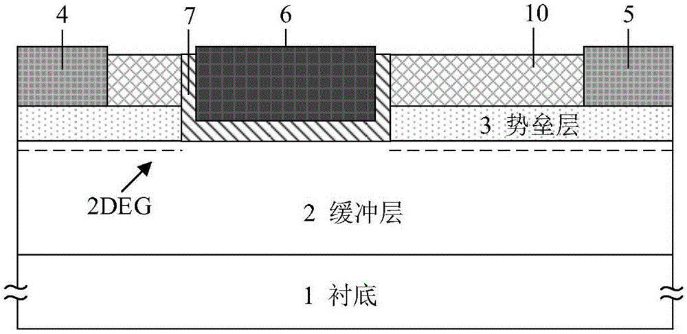
[0039] Such as Figure 6 As shown, the difference between this example and Example 1 is that the isolation layer 11 uses grooves to block 2DHG, which is used to avoid premature breakdown of the device caused by the leakage current of the gate-2DHG-2DEG when the gate is applied with a positive voltage. .


PUM


Abstract

The invention belongs to the technical field of a semiconductor and specifically relates to an HEMT device with a junction type semiconductor layer. The device is mainly constructed in such a way that the junction type semiconductor layer is grown on the upper surface of a barrier layer between a grid and a drain and the junction type semiconductor layer and the barrier layer form two-dimensional cavity gas (2DHG). On one hand, grid metal and the junction type semiconductor layer form a rectification structure so that leakage currents of grid-2DHG-2DEG caused when the grid is positively pressurized are avoided, and at the same time, a separating layer is employed between a drain electrode and the junction type semiconductor layer for blocking the 2DHG; and on the other hand, the 2DHG between the grid and the drain and the 2DEG form polarized super junctions, in case of a blocking state, a drift region is exhausted under assistance, the electric field concentration effect of the end, nearby the drain, of the grid of the device is effectively improved, at the same time, a new electric field peak is introduced to the contact portion between a P-type doping area and an N-type doping area, electric field distribution on the surface of the device is enabled to be more uniform, and breakdown voltage of the device at a switching-off state is improved. The HEMT device with the junction type semiconductor layer is especially suitable for an HEMT device.

Description

technical field [0001] The invention belongs to the technical field of semiconductors, and in particular relates to a HEMT (High Electron Mobility Transistor, High Electron Mobility Transistor) device with a junction semiconductor layer. Background technique [0002] The wide bandgap semiconductor gallium nitride (GaN) has the characteristics of high critical breakdown electric field (~3.3×10⁶V / cm), high electron mobility (~2000cm2 / V s), and the heterojunction based on GaN material has high electronic The mobility transistor (HEMT) also has a high-concentration (~1013cm-2) two-dimensional electron gas (2DEG) channel, which makes GaNHEMT devices have high reverse blocking voltage, low forward conduction resistance, and high operating frequency. The application field of high current, low power consumption and high voltage switching devices has great application prospects. [0003] The key to power switching devices is to achieve high breakdown voltage, low on-resistance and h...

Claims


Application Information

Patent Timeline
Patent Type & Authority Applications(China)
IPC IPC(8): H01L29/778H01L29/40
CPCH01L29/402H01L29/7783
Inventor 罗小蓉杨超熊佳云魏杰吴俊峰彭富张波
Owner UNIV OF ELECTRONICS SCI & TECH OF CHINA
Why Eureka
Try Eureka