Low-temperature polycrystalline silicon thin film transistor and preparation method thereof

A technology of thin-film transistors and low-temperature polysilicon, which is applied in transistors, semiconductor/solid-state device manufacturing, semiconductor devices, etc., and can solve problems such as low production efficiency, increased process complexity, and high manufacturing costs

Active Publication Date: 2015-12-09
TRULY HUIZHOU SMART DISPLAY
View PDF4 Cites 12 Cited by
  • Summary
  • Abstract
  • Description
  • Claims
  • Application Information

AI Technical Summary

Problems solved by technology

[0009] However, when the low-temperature polysilicon thin film transistor is prepared by the above-mentioned traditional process, it needs to go through multiple processes such as photoresist coating, mask exposure, development and etching, which increases the complexity of the process, and the manufacturing cost is high. low efficiency

Method used


Image

  • Low-temperature polycrystalline silicon thin film transistor and preparation method thereof
  • Low-temperature polycrystalline silicon thin film transistor and preparation method thereof
  • Low-temperature polycrystalline silicon thin film transistor and preparation method thereof

Examples


preparation example Construction

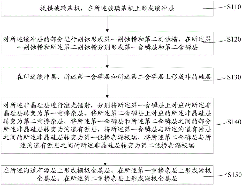
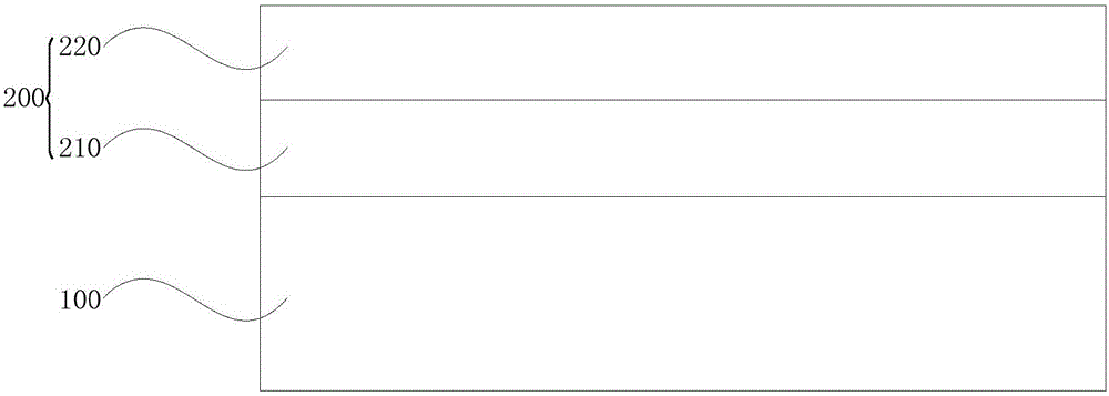
[0036] like figure 1 As shown, the method for preparing a low-temperature polysilicon thin film transistor according to an embodiment of the present invention includes the following steps:

[0037] S110: Provide a glass substrate, and form a buffer layer on the glass substrate.

[0038] In practical applications, the glass substrate needs to have high transparency, low reflectivity, good thermal stability and corrosion resistance, high mechanical strength and good mechanical processing characteristics. In addition, the glass substrate also Good electrical insulation is required. Preferably, the glass substrate is borosilicate glass or alkali-free aluminosilicate glass without alkali ions.

[0039] In order to prevent the metal ions in the glass substrate from entering the amorphous silicon layer during the deposition process of the amorphous silicon layer, for example, the forming of the protective insulating layer buffer layer on the glass substrate specifically includes th...


PUM

PropertyMeasurementUnit
thicknessaaaaaaaaaa
lengthaaaaaaaaaa

Abstract

A low-temperature polycrystalline silicon thin film transistor and a preparation method thereof. The method includes: etching part of a buffer layer to form a first etching groove and a second etching groove, and forming a first phosphorus-containing layer and a second phosphorus-containing layer in the first etching groove and the second etching groove; forming amorphous silicon layers on the buffer layer, the first phosphorus-containing layer and the second phosphorus-containing layer; and performing laser radiation on the amorphous silicon layer, converting the corresponding amorphous silicon layer on the first phosphorus-containing layer into a first heavily-doped layer, converting the corresponding amorphous silicon layer on the second phosphorus-containing layer into a second heavily-doped layer, converting part of the amorphous silicon layer between the first phosphorus-containing layer and the second phosphorus-containing layer into a channel active layer, converting the amorphous silicon layer between the first phosphorus-containing layer and the channel active layer into a first lightly-doped drain end, and converting the amorphous silicon layer between the second phosphorus-containing layer and the channel active layer into a second lightly-doped drain end. The abovementioned preparation method adopts a high-temperature diffusion type doping principle, and has the advantages of relatively simple technological process and relatively high production efficiency.

Description

technical field [0001] The invention relates to the technical field of preparation of low-temperature polysilicon thin film transistors, in particular to a low-temperature polysilicon thin film transistor and a preparation method thereof. Background technique [0002] With the continuous development of products such as smart phones, tablet computers and televisions, displays using low-temperature polysilicon thin film transistors have also been more and more widely used, for example, AMOLED (Active-matrix organic light emitting diode, active matrix organic light emitting diode or active Matrix organic light emitting diodes. [0003] At present, low-temperature polysilicon thin film transistors are mainly prepared by the following steps. [0004] Provide glass substrate; [0005] Sequential SiN on glass substrate x (silicon nitride) layer and SiO x (silicon oxide) layer to form an isolation layer; [0006] An a-Si (amorphous silicon) layer is formed on the isolation laye...

Claims


Application Information

Patent Timeline
Patent Type & Authority Applications(China)
IPC IPC(8): H01L21/336H01L29/786
CPCH01L29/66757H01L29/78675
Inventor 陈卓
Owner TRULY HUIZHOU SMART DISPLAY
Why Eureka
Try Eureka