Passivated emitter region back surface partial diffused crystalline silicon solar cell preparation method

A solar cell, passivation emission technology, applied in the field of solar cells, can solve problems such as poor utilization of sunlight energy, low reflectivity, and decrease in reverse saturation current density

Active Publication Date: 2015-12-23
ZHEJIANG AIKO SOLAR ENERGY TECH CO LTD +1
View PDF3 Cites 1 Cited by
  • Summary
  • Abstract
  • Description
  • Claims
  • Application Information

AI Technical Summary

Problems solved by technology

The structure design of the battery is relatively simple, resulting in technical problems that cannot greatly improve the photoelectric conversion efficiency of the battery. For example, the energy of sunlight cannot be well utilized, forming a so-called "dead layer"
The metal electrode on the front surface cannot be made very narrow, otherwise it will block the effective absorption of light in the silicon wafer, the single diffusion technology cannot effectively solve the problems of electrode contact

Method used


Image

  • Passivated emitter region back surface partial diffused crystalline silicon solar cell preparation method

Examples


Embodiment Construction

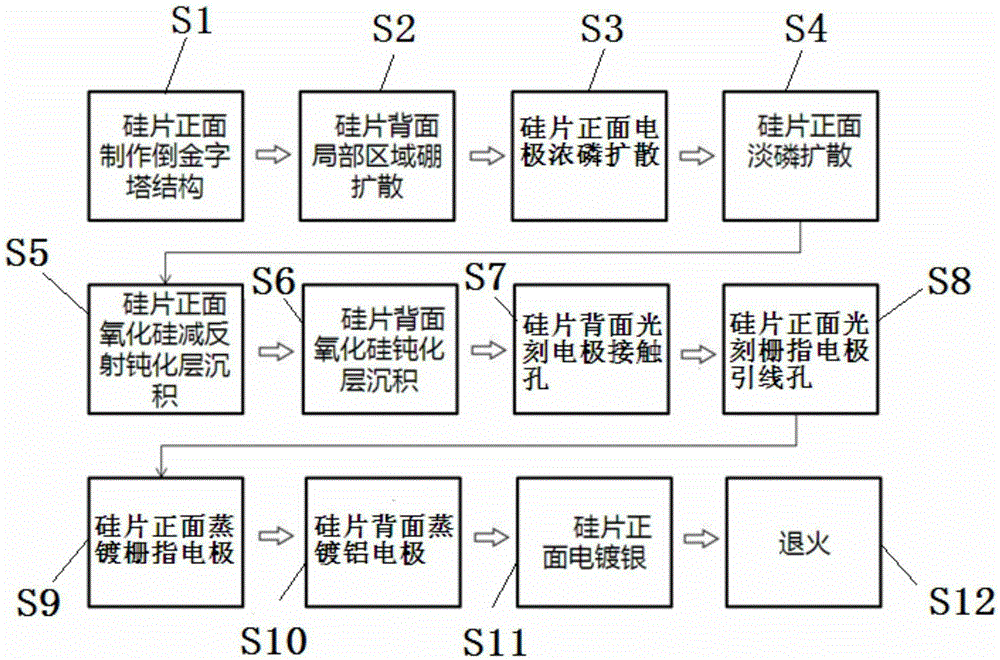
[0033] Such as figure 1 A method for preparing a partially diffused crystalline silicon solar cell on the back side of a passivated emission region comprises the following steps: step S1: making an inverted pyramid structure on the front side of the silicon wafer; step S2: diffusion of boron in a local area on the back side of the silicon wafer; step S3: silicon wafer Diffusion of concentrated phosphorus on the front electrode; step S4: light phosphorus diffusion on the front side of the silicon wafer; step S5: deposition of a silicon oxide anti-reflection passivation layer on the front side of the silicon wafer; step S6: deposition of a silicon oxide passivation layer on the back side of the silicon wafer; step S7: the back side of the silicon wafer Photoetching electrode contact holes; step S8: photoetching grid finger electrode lead holes on the front side of the silicon wafer; step S9: evaporating grid finger electrodes on the front side of the silicon wafer; step S10: evap...


PUM


Abstract

The invention discloses a passivated emitter region back surface partial diffused crystalline silicon solar cell preparation method. The method includes the following steps of: silicon wafer front surface inverted pyramid structure production; silicon wafer back surface partial region boron diffusion; silicon wafer front surface gate interdigital electrode heavy phosphorous diffusion; silicon wafer front surface light phosphorus diffusion; silicon wafer front surface silicon oxide (SiO2) anti-reflection passivation layer deposition; silicon wafer back surface silicon oxide (SiO2) passivation layer deposition; silicon wafer back surface electrode contact hole photoetching; silicon wafer front surface gate interdigital electrode lead hole photoetching, silicon wafer front surface gate interdigital electrode evaporation; silicon wafer back surface aluminum electrode evaporation; silicon wafer front surface electrosilvering and annealing; and solar cell formation. With the method of the invention adopted, the front surface of a cell is of an inverted pyramid structure, and the light receiving effect of the cell is better than that of an ordinary texturized surface structure, and the cell has very low reflectivity, and therefore, the Jsc of the cell can be improved.

Description

technical field [0001] The invention relates to the technical field of solar cells, in particular to a method for preparing a partially diffused crystalline silicon solar cell on the back of a passivated emission region. Background technique [0002] A solar cell is a device that effectively absorbs solar radiation energy and uses the photovoltaic effect to convert light energy into electrical energy. When sunlight shines on a semiconductor P-N junction (P-NJunction), a new hole-electron pair (V -Epair), under the action of the P-N junction electric field, holes flow from the N region to the P region, electrons flow from the P region to the N region, and a current is formed after the circuit is turned on. Because it is a solid semiconductor device that converts sunlight energy into electrical energy by using the photovoltaic effect of various potential barriers, it is also called a solar cell or a photovoltaic cell, and is an important component of a solar array power system...

Claims


Application Information

Patent Timeline
IPC IPC(8): H01L31/18H01L31/0236H01L31/0216H01L31/0224H01L21/22
CPCH01L21/22H01L31/02168H01L31/022425H01L31/0236H01L31/18Y02E10/50Y02P70/50
Inventor 秦崇德方结彬石强黄玉平何达能陈刚
Owner ZHEJIANG AIKO SOLAR ENERGY TECH CO LTD
Why Eureka
Try Eureka