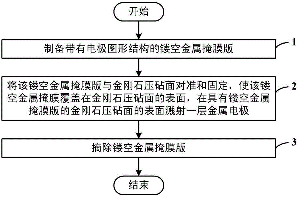
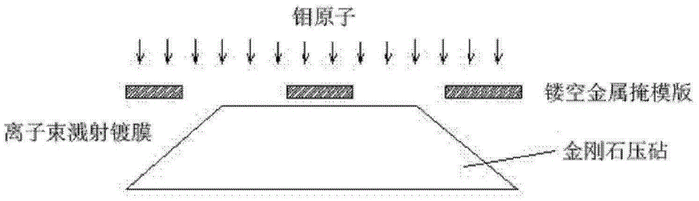
Method for preparing metal electrode on diamond anvil cell
A diamond anvil and metal electrode technology, applied in metal material coating technology, circuits, electrical components, etc., can solve the problems of large error, difficult operation, small anvil surface, etc., and achieve easy operation, simple operation and simple process Effect
- Summary
- Abstract
- Description
- Claims
- Application Information
AI Technical Summary
Problems solved by technology
Method used
Image

Examples
Embodiment 1
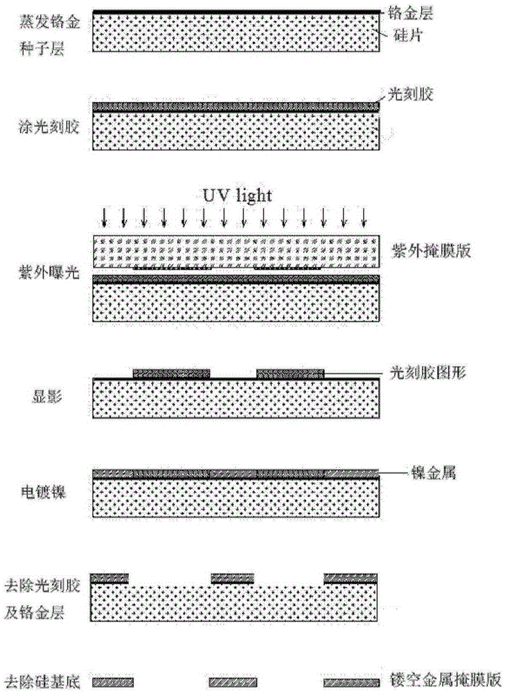
[0034] refer to Figure 2 to Figure 4 , the method for preparing a metal electrode on a diamond anvil provided in Example 1 of the present invention will be described in detail below.
[0035] The first step is to prepare a hollow metal mask. The hollow metal mask is a nickel metal sheet, which is composed of a hollow area and a solid area. The hollow area is the required hollow electrode pattern, the solid area is nickel metal, and the area other than the pattern belongs to the nickel metal solid area. Its preparation method is as figure 2 As shown, it includes: (1) preparing a chromium-gold seed layer with a thickness of 10 nanometers on the surface of a cleaned polished silicon wafer by thermal evaporation. (2) Spin-pattern photoresist (4620) on the surface at 1000 rpm, pre-baked at 90 degrees for 30 minutes, with a thickness of 25 microns, and exposed to the ultraviolet lithography machine for 200 seconds, at a concentration of 7.5 parts per thousand of hydrogen Develo...
Embodiment 2
[0039] The method for preparing a metal electrode on a diamond anvil provided by Example 2 of the present invention will be described in detail below.
[0040] In step 1, a chromium-gold seed layer with a thickness of 10 nanometers is prepared on the surface of the silicon wafer by thermal evaporation.
[0041] Step 2, apply photoresist (4620) on the surface of the silicon wafer in step 1 by spin coating at 1000 rpm, pre-bake at 90°C for 30 minutes, and the thickness of the photoresist is 25 microns.
[0042] Step 3, covering the surface of the silicon wafer coated with photoresist with the ultraviolet lithography mask plate with the electrode pattern, exposing the ultraviolet lithography machine for 60 seconds, and developing for 5 minutes with 7.5 / 1000 sodium hydroxide developer solution, A photoresist electrode pattern is obtained on the surface of the silicon wafer.
[0043] Step 4, electroplating nickel metal with a thickness of 20 microns on the surface of the silicon waf...
PUM
| Property | Measurement | Unit |
|---|---|---|
| Diameter | aaaaa | aaaaa |
| Thickness | aaaaa | aaaaa |
Abstract
Description
Claims
Application Information