A kind of method adopting plasma method to prepare nano metal silicon

A nano-metal silicon and plasma technology, applied in the direction of silicon, etc., can solve the problems that cannot meet the requirements of aerospace, metal silicon nano-particle crystal defects, and short service life of electronic components, and achieve low production cost and no crystal lattice. Effect of defects, narrow particle size distribution

Inactive Publication Date: 2017-10-03
NEIJIANG NORMAL UNIV
View PDF4 Cites 0 Cited by
  • Summary
  • Abstract
  • Description
  • Claims
  • Application Information

AI Technical Summary

Problems solved by technology

However, the crushing method causes defects such as crystal defects, irregular structure and shape, and wide particle size distribution of metal silicon nanoparticles, which leads to short service life of electronic components, especially unable to meet the requirements of aerospace.

Method used


Image

  • A kind of method adopting plasma method to prepare nano metal silicon

Examples


Embodiment

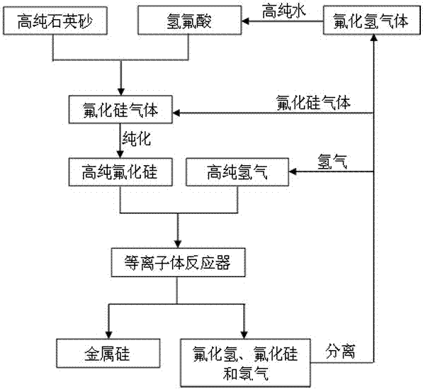
[0027] The present embodiment provides a kind of method adopting plasma method to prepare nano-metal silicon, it comprises the following steps:

[0028] A. 10g of quartz sand and 150mL of hydrofluoric acid with a mass content of 10% to 50% are reacted to generate silicon fluoride gas;

[0029] B. Purifying and removing impurities from the silicon fluoride gas prepared in step A to obtain high-purity silicon fluoride gas (mass content ≥ 98.5%);

[0030] C. Completely mix the high-purity silicon fluoride gas obtained in step B with hydrogen in a metered volume ratio of 1:4; then pass the mixed gas into the plasma reactor at a flow rate of 50mL / min for reaction to generate metal Silicon nanoparticles (particle size ≤ 50nm) and hydrogen fluoride gas;

[0031] D. Separating and purifying the mixture of unreacted silicon fluoride, hydrogen and generated hydrogen fluoride gas through a separator to obtain qualified high-purity silicon fluoride (mass content ≥ 98.5%) and hydrogen (ma...


PUM

PropertyMeasurementUnit
particle diameteraaaaaaaaaa

Abstract

The invention provides a method for preparing nanometer metal silicon by using a plasma method, which belongs to the technical field of metal silicon preparation and comprises the following steps in sequence: preparing silicon fluoride gas, purifying silicon fluoride gas and preparing nanometer metal silicon. The method prepares silicon fluoride gas by reacting quartz sand with hydrofluoric acid in step A; then purifies the silicon fluoride gas in step B; and finally makes the purified silicon fluoride molecules and hydrogen molecules in the plasma through step C Under the action of the body, it is activated and reacted to prepare nano-metal silicon. Therefore, compared with the existing improved Siemens method and cold hydrogenation method to prepare metal silicon, the method for preparing nano-metal silicon by plasma method has the advantages of simple preparation process, easy operation, low energy consumption and production cost; The nano-metal silicon has a complete crystal structure, no lattice defects, and a narrow particle size distribution. It can meet the quality requirements of the microelectronics industry for electronic-grade metal silicon without crushing methods.

Description

technical field [0001] The invention relates to the technical field of preparing metal silicon, in particular to a method for preparing nanometer silicon metal by using a plasma method. Background technique [0002] The existing metal silicon is mainly produced by the improved Siemens method and the cold hydrogenation method, which has the disadvantages of complex process, serious environmental pollution, large equipment investment, high energy consumption and high production cost. The product quality of solar-grade and electronic-grade metal silicon produced by these two processes depends on the impurity content of the raw gas trichlorosilane, such as iron, aluminum, calcium, boron and phosphorus. In the industry, multi-stage rectification is commonly used to remove the impurities of trichlorosilane. The impurity removal effect of rectification in actual production cannot meet the requirements of metal silicon for impurity content. The impurity brought in and the rectifica...

Claims


Application Information

Patent Timeline
Patent Type & Authority Patents(China)
IPC IPC(8): C01B33/03
Inventor 郑小刚霍峰刘勇黄敏宋玉春王姝羡
Owner NEIJIANG NORMAL UNIV
Why Eureka
Try Eureka