Dielectrically isolated integrated circuit extending wafer and preparation method thereof

A dielectric isolation and integrated circuit technology, applied in the field of dielectric isolation epitaxial wafers and its preparation, can solve the problems of parasitic radiation resistance, poor isolation performance, and no performance, and achieve shortening of high temperature time, high temperature resistance and radiation resistance Performance improvement, the effect of improving circuit performance

Inactive Publication Date: 2009-05-06
TIANSHUI HUATIAN MICROELECTRONICS
View PDF0 Cites 2 Cited by
  • Summary
  • Abstract
  • Description
  • Claims
  • Application Information

AI Technical Summary

Problems solved by technology

In this process, the isolation performance deteriorates with the increase of temperature. The PNP tube can only be made into a horizontal PNP tube. The performance is not as good as that of the vertical PNP tube. There are parasitic effects and poor radiation resistance, which affects the application in some special requirements. application

Method used


Image

  • Dielectrically isolated integrated circuit extending wafer and preparation method thereof
  • Dielectrically isolated integrated circuit extending wafer and preparation method thereof
  • Dielectrically isolated integrated circuit extending wafer and preparation method thereof

Examples


Embodiment 1

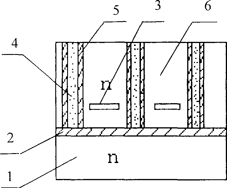
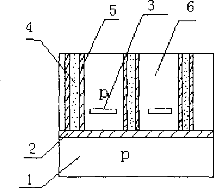
[0041] Example 1, see figure 1 , an N-type dielectric isolation integrated circuit epitaxial wafer, including a substrate material N-type single crystal silicon 1, on which a sandwich oxide layer 2 is arranged, and an N-type silicon epitaxial layer 6, which is provided in the silicon epitaxial layer 6. There is a buried layer 3; its silicon epitaxial layer 6 is separated into isolated squares insulated from each other by silicon dioxide 5, polysilicon 4 and sandwich oxide layer 2. The thickness of the N-type silicon epitaxial layer 6 is 0.5-16 μm; the sheet resistance of the buried layer 3 is 10-15Ω / □ for the N-type and 8-20Ω / □ for the P-type.

Embodiment 2

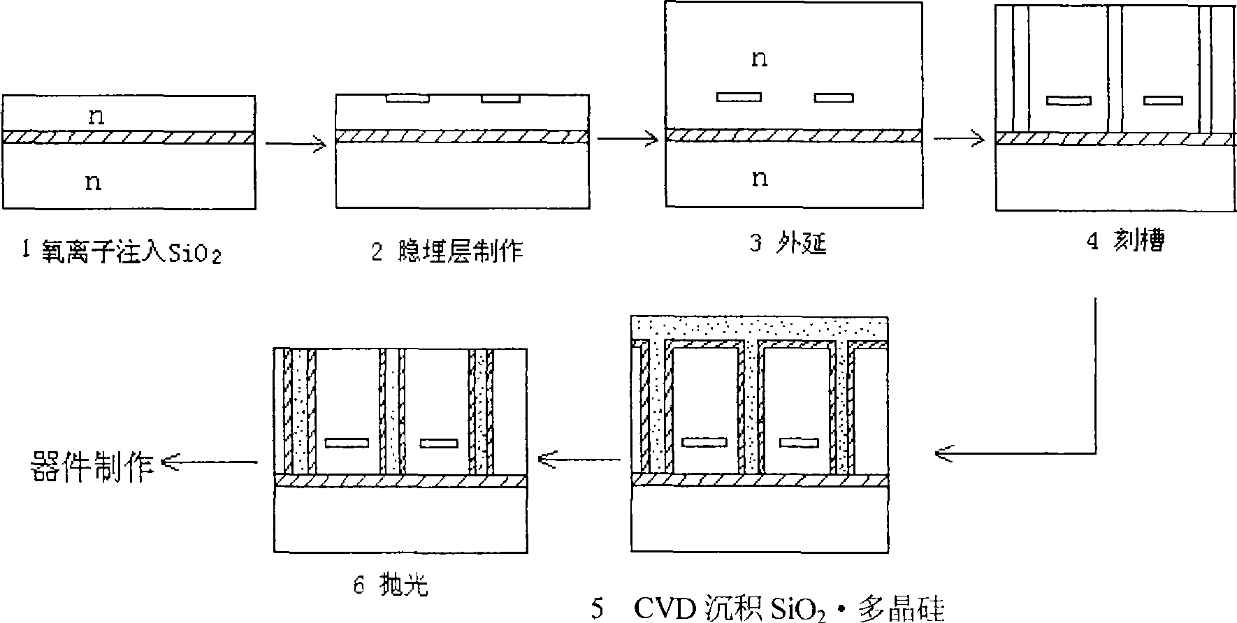
[0043] Example 2, see figure 2 , a preparation method of an N-type dielectric isolation integrated circuit epitaxial wafer, the preparation steps are:

[0044] (1) Preparation of silicon SOI silicon wafers on insulators: Oxygen ions are implanted on the surface of N-type 2-4Ωcm polished single crystal silicon wafers, and annealed at a high temperature at a temperature of 25-1200°C to form a sandwich oxide layer with a depth of 2-4μm; During implantation, the substrate temperature is 400-700℃, the implantation energy is 150-200kev, and the dose is 10 17 -10 18 / cm 2 :

[0045] (2) Preparation of low-resistance buried layer: in the above step (1), the surface of the SOI silicon wafer is oxidized first, then photolithography is performed, and then a local high concentration of arsenic is performed 8×10 19 -10 20 / cm 3 Ion implantation, after high temperature annealing, the temperature is 25-1200℃, the sheet resistance is controlled at 10-15Ω / □, and the junction depth is co...

Embodiment 3

[0051] Embodiment 3, the preparation method of the N-type dielectric isolation integrated circuit epitaxial wafer, the preparation step (2) also includes: forming N + After the buried layer, the local high concentration of boron is 2-5×10 19 / cm 3 Ion implantation, after high temperature annealing, the temperature is 25-1200 ℃, the sheet resistance is controlled at 8-20Ω / port, and the junction depth is controlled at 2.0-3.0μm; the formation of P + Buried layer, the implantation process substrate temperature is 400-700℃, the implantation energy is 100-150kev, and the dose is 10 15 -10 16 / cm 2 . The rest of the steps are the same as in Example 1.


PUM


Abstract

The invention mainly relates to a dielectric isolation epitaxial wafer and a preparation method thereof. The N-shaped / P-shaped dielectric isolation integrated circuit epitaxial wafer comprises N-shaped / P-shaped monocrystalline silicon (1) with backing material. A sandwich oxide layer (2) is arranged on the monocrystalline silicon (1). The invention is mainly characterized in that the dielectric isolation epitaxial wafer further comprises an N-shaped / P-shaped silicon epitaxial layer (6); a buried layer (3) is arranged in the silicon epitaxial layer (6); the silicon epitaxial layer (6) is divided into mutually-insulating isolation blocks by silicon dioxide (5), polysilicon (4) and the sandwich oxide layer (2). The invention also discloses a preparation method of the N-shaped / P-shaped dielectric isolation integrated circuit epitaxial wafer. The preparation method comprises the following steps: preparing a silicon chip on an insulating body, preparing the buried layer with low resistance, extending outwardly, notching, growing the silicon dioxide and the polysilicon, and polishing. Because the high temperature time is shortened greatly during the preparation, the invention has the advantages of more complete crystal structure and more accurate process control, and can be used for manufacturing circuits with high performance and special requirements.

Description

Technical field: [0001] The invention mainly relates to a dielectric isolation epitaxial wafer and a preparation method thereof. It belongs to the technical field of integrated circuits. Background technique: [0002] In the manufacture of bipolar analog and digital integrated circuits, a monolithic PN junction isolation epitaxial wafer method is generally used. Except for the vertical PNP tube of the output substrate, the other PNP tubes can only be made into horizontal PNP tubes, and the performance is not as good as that of vertical PNP tubes. In the case of higher reliability requirements and harsher working environment conditions, the circuits manufactured by the PN junction isolation epitaxy method are limited to a certain extent, and the performance of the analog integrated circuits manufactured by the dielectric isolation epitaxial wafer is obviously better than the former. With the development of human beings to deep space exploration, the requirements for radiati...

Claims


Application Information

Patent Timeline
Patent Type & Authority Applications(China)
IPC IPC(8): H01L27/12H01L21/84H01L21/76
Inventor 周鸣新
Owner TIANSHUI HUATIAN MICROELECTRONICS
Why Eureka
Try Eureka