LDMOS device manufacturing method

A manufacturing method and device technology, applied in semiconductor devices, electrical components, circuits, etc., can solve the problems of unsuitability for extended gates, poor experimental repeatability, affecting the electrical properties of extended gates, etc. The effect of reducing production costs

Active Publication Date: 2016-02-03
UNIV OF ELECTRONICS SCI & TECH OF CHINA
View PDF5 Cites 4 Cited by
  • Summary
  • Abstract
  • Description
  • Claims
  • Application Information

AI Technical Summary

Problems solved by technology

[0004] Compared with single crystal silicon, polysilicon has disadvantages such as large leakage current and poor experiment repeatability, which will affect the electrical performance of the extended gate, so polysilicon is not suitable for making extended gates

Method used


Image

  • LDMOS device manufacturing method
  • LDMOS device manufacturing method
  • LDMOS device manufacturing method

Examples


Embodiment 1

[0050] The manufacturing process of the LDMOSFT device in this example is as follows:

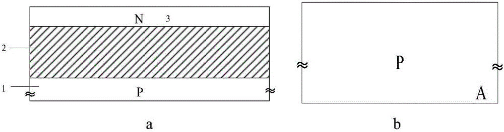
[0051] The first step: preparing SOI material: the SOI material includes a substrate layer 1, a dielectric buried layer 2 and an active layer 3, wherein the conductivity type of the substrate layer 1 is not limited, and the conductivity type of the active layer 3 is the first conductivity type, The dielectric buried layer 2) is located between the substrate layer 1 and the active layer 3 (such as figure 1 as shown in a);

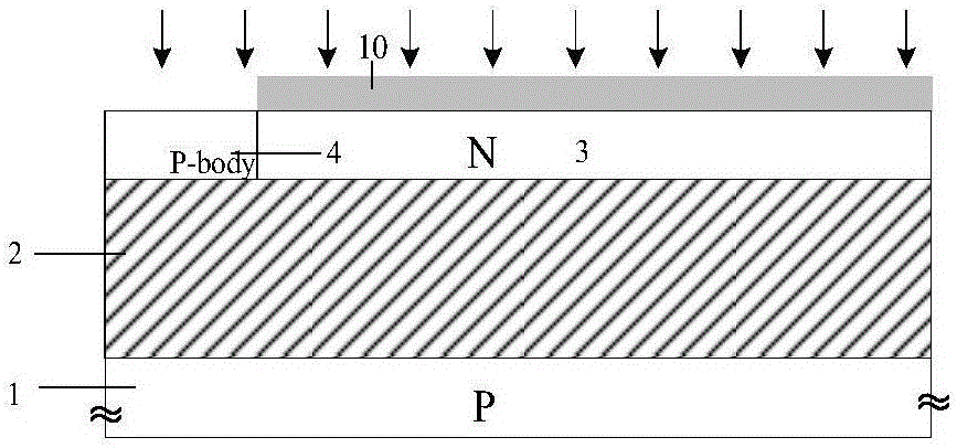
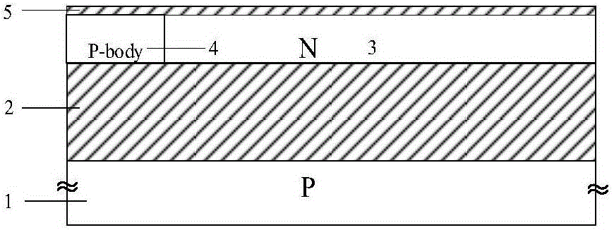
[0052] The second step: adopt ion implantation process on the above SOI material, implant the second conductivity type impurity in the active layer 3, and form the second conductivity type body region 4 (such as figure 2 shown), and then thermally oxidized on top of the active layer 3 to form a dielectric isolation layer 5 (such as image 3 shown);

[0053] The third step: in another second conductivity type semiconductor material A (such as figure 1 As shown in b) t...

Embodiment 2

[0061] The difference between this example and Example 1 is that

[0062] The fifth step is: use an etching process to etch the two ends of the auxiliary semiconductor layer 6 to the upper surface of the active layer 3 to form a first active region window and a second active region window. A gate dielectric 11 is grown on the upper surface of the active region window and the second active region window, such as Figure 12 As shown, polysilicon 12 is deposited on the upper surface of part of the gate dielectric 11 located on the upper surface of the semiconductor body region 4 of the second conductivity type and connected to the auxiliary semiconductor layer 6, and the polysilicon gate is formed after etching the polysilicon 12 and the gate dielectric 11, as shown in FIG. Figure 13 shown;

[0063] The eighth step is: making a source metal in the first active region window, with a passivation layer dielectric 9 between the source metal and the gate contact region 82; making a ...

Embodiment example 3

[0066] The difference between this example and Example 2 is that

[0067] There is a gate dielectric 11 between the formed polysilicon gate and the auxiliary semiconductor layer 4, such as Figure 14 shown;

[0068] The seventh step also includes: implanting semiconductor impurities of the second conductivity type into the part of the auxiliary semiconductor layer 4 connected to the gate dielectric 11 to form a second gate contact region 84, such as Figure 15 shown;

[0069] The eighth step further includes: forming a second source metal on the upper surface of the second gate contact region 84 .

[0070] The first doping type and the second doping type of the semiconductor are opposite doping types. When the first doping type is n-type doping, the second doping type is p-type doping; correspondingly , when the first doping type is p-type doping, the second doping type is n-type doping.


PUM


Abstract

The invention belongs to the semiconductor technology, and particularly relates to an LDMOS device manufacturing method. The LDMOS device manufacturing method mainly comprises steps: a semiconductor active layer of a first conductive type grows on the upper surface of a semiconductor substrate of a second conductive type; bonding and stripping are carried out on the upper layer of the semiconductor active layer of the first conductive type to form a dielectric barrier layer, and an auxiliary semiconductor layer is formed on the semiconductor active layer of the first conductive type on the upper surface of the dielectric barrier layer; semiconductor impurities of a second conductive type are injected in the auxiliary semiconductor layer; two ends of the auxiliary semiconductor layer are etched to the surface of the dielectric barrier layer to form a first active region window and a second active region window; a body region is manufactured in the first active region window, and a source metal grows; and a drain contact region is manufactured in the second active region window, and a drain metal grows. The LDMOS device manufacturing method has the beneficial effects that an extended gate can be ensured to be a monocrystalline silicon material, and influences on electrical performance of an extended gate device by a poly gate can be avoided.

Description

technical field [0001] The present invention relates to the field of power semiconductor device manufacturing, more specifically, the present invention relates to a kind of LDMOS (Lateral Double-diffusion Metal Oxide Semiconductor field effect transistor, lateral double-diffusion metal-oxide-semiconductor field effect transistor) device manufacturing method. Background technique [0002] Compared with VDMOS (VerticalDouble-diffused MOSFET, vertical double-diffused metal-oxide-semiconductor field-effect transistor), LDMOS has the characteristics of fast switching speed and easy integration. Therefore, LDMOS is widely used in power integrated circuits, especially in radio frequency circuits. [0003] For conventional LDMOS, the specific on-resistance R on,sp There is a contradictory relationship between (specific on-resistance = on-resistance x device area) and withstand voltage BV: R on,sp ∝BV 2.5 . Reducing the doping concentration of the drift region and increasing the ...

Claims


Application Information

Patent Timeline
Patent Type & Authority Applications(China)
IPC IPC(8): H01L29/66H01L21/28
CPCH01L29/401H01L29/42356H01L29/42364H01L29/66681
Inventor 罗小蓉张彦辉刘建平谭桥尹超魏杰周坤吕孟山田瑞超张波
Owner UNIV OF ELECTRONICS SCI & TECH OF CHINA
Why Eureka
Try Eureka