A kind of semiconductor element and its preparation method

A semiconductor and component technology, applied in the field of semiconductor components and their preparation, can solve problems such as inconsistency in the ability to release stress, damage to the performance of semiconductor devices, and poor compactness of the aluminum nitride layer, so as to avoid cracks and pores and reduce device leakage phenomenon, the effect of reducing lattice differences

Active Publication Date: 2018-07-10
ANHUI SANAN OPTOELECTRONICS CO LTD
View PDF4 Cites 0 Cited by
  • Summary
  • Abstract
  • Description
  • Claims
  • Application Information

AI Technical Summary

Problems solved by technology

However, at present, the physical vapor deposition method is used to directly grow aluminum nitride on the surface of silicon substrates, and it is easy to form an amorphous silicon oxide layer at the interface between the substrate and aluminum nitride, resulting in the deterioration of the quality of the subsequently formed aluminum nitride layer, resulting in the following Problem: The aluminum nitride layer is used as a stress buffer layer, and its ability to release stress is inconsistent, and the stress is concentrated on the amorphous silicon nitride layer on the interface, which is easy to cause cracks and destroy the quality of the entire semiconductor device; the aluminum nitride layer The densification becomes poor, and pores are formed. Then, when the gallium-containing nitride is deposited in the chemical vapor phase, the gallium element directly corrodes the silicon substrate through the pores, forming pits, and destroying the performance of the entire semiconductor device.

Method used


Image

  • A kind of semiconductor element and its preparation method
  • A kind of semiconductor element and its preparation method
  • A kind of semiconductor element and its preparation method

Examples


Embodiment 1

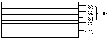
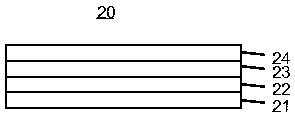
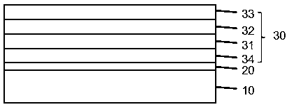
[0034] See attached Figure 1~2 , the present embodiment provides a semiconductor element, which includes: a silicon substrate 10, a multi-layer buffer structure 20 and an epitaxial functional layer 30, where the epitaxial functional layer 30 is a first semiconductor layer 31, a light emitting layer 32 and a second The light-emitting diode epitaxial layer composed of two semiconductor layers 33; the first semiconductor layer 31 and the second semiconductor layer 33 are respectively a semiconductor layer doped with donor impurities and a semiconductor layer doped with acceptor impurities. Of course, the non-doped semiconductor layer 34 can also be included in the semiconductor element of the present invention (see the attached image 3 ). The multi-layer buffer structure 20 consists of an aluminum metal protective layer 21 with a thickness of 1-100 angstroms, an aluminum oxide metal oxide protective layer 22 with a thickness of 1-500 angstroms, and an oxygen-doped aluminum nit...

Embodiment 2

[0044] See attached Figure 4 The difference between this embodiment and Embodiment 1 is that a transistor epitaxial layer is deposited on the surface of the multilayer buffer structure 20 as an epitaxial functional layer 30 to form a transistor element. The preparation method and structure are as follows: the aluminum metal protection layer 21, the oxide The substrate of the multilayer buffer structure 20 composed of the aluminum metal oxide protection layer 22, the oxygen-doped aluminum nitride transition layer 23 and the oxygen-doped aluminum nitride buffer layer 24 is transferred into the MOCVD chamber, and aluminum gallium nitride is deposited by the MOCVD method layer 35 to further buffer the lattice stress of the multilayer buffer structure 20 to avoid cracks; then another layer 36 of gallium nitride semiconductor layer 36 that is not intentionally doped or doped with carbon or doped with iron, and then deposited aluminum gallium nitride semiconductor Layer 37, the AlGa...


PUM

PropertyMeasurementUnit
thicknessaaaaaaaaaa
thicknessaaaaaaaaaa
thicknessaaaaaaaaaa

Abstract

The invention provides a semiconductor element, which avoids the formation of an amorphous layer on the surface of a silicon substrate by using a metal protective layer and a metal oxide protective layer grown on a substrate; and uses a transition layer to reduce the difference between the metal oxide protective layer and the metal oxide protective layer. The crystal lattice difference of the III-IV group buffer layer improves the crystal quality of the III-IV group buffer layer. The present invention also proposes a preparation method, which can avoid the formation of an amorphous layer near the interface of the silicon substrate and avoid the generation of cracks. At the same time, the high-quality multi-layer buffer structure deposited by PVD method is fully utilized, and gallium nitride or indium gallium nitride or aluminum gallium nitride epitaxial layers are grown on it to make light-emitting diode elements or transistor elements.

Description

technical field [0001] The invention belongs to the technical field of semiconductors, in particular to a semiconductor element and a preparation method thereof. Background technique [0002] The physical vapor deposition method (PVD method) has the characteristics of simple process, less environmental pollution, less raw material consumption, uniform and dense film formation, and strong bonding with the substrate. It is currently being increasingly used in the preparation of semiconductor components. Among them, it is usually used for the preparation of the bottom layer, such as depositing an aluminum nitride layer as a buffer layer, which can reduce and buffer defects and stresses caused by lattice mismatch and thermal mismatch between the substrate and the epitaxial layer, and improve semiconductor performance. Component quality. [0003] Compared with chemical vapor deposition, the atoms sputtered by PVD method have higher energy (generally 10~20eV) and stronger migrati...

Claims


Application Information

Patent Timeline
Patent Type & Authority Patents(China)
IPC IPC(8): H01L21/02H01L29/20
CPCH01L21/02381H01L21/02455H01L21/02491H01L21/02505H01L21/02631H01L29/20H01L21/02H01L33/007H01L33/12H01L33/32H01L21/02172H01L21/022H01L29/0653H01L33/005H01L33/02H01L33/44
Inventor 徐志波周圣伟程志青王肖
Owner ANHUI SANAN OPTOELECTRONICS CO LTD
Why Eureka
Try Eureka