Patterned substrate, preparation method and light-emitting diode

A patterned substrate and light-emitting diode technology, applied in semiconductor devices, electrical components, circuits, etc., can solve problems affecting crystal performance, uneven surface of the buffer layer, affecting device performance, etc., to reduce lattice defect density, reduce Small growth chance, effect of improving crystal quality

Inactive Publication Date: 2016-02-24
ANHUI SANAN OPTOELECTRONICS CO LTD
View PDF7 Cites 15 Cited by
  • Summary
  • Abstract
  • Description
  • Claims
  • Application Information

AI Technical Summary

Problems solved by technology

However, due to the large lattice mismatch between the widely used sapphire substrate and the gallium nitride-based material layer, nucleation and growth are difficult, and in order to overcome the problem of difficult nucleation, it was proposed to heat the substrate at about 1000 °C Finally, grow a low-quality low-temperature buffer layer, and then turn to high-temperature conditions to grow high-quality GaN-based epitaxial layers
Due to the high and low temperature conversion in this process, the efficiency of the MOCVD machine is reduced; at the same time, the large temperature difference between different layers increases the stress between different layers, thus affecting the crystal performance.
[0003] Therefore, it has been proposed to deposit a layer of aluminum nitride on the surface of the patterned substrate to reduce the lattice difference between the substrate and the GaN-based epitaxial layer. The current common process is to place the patterned substrate on PVD The aluminum nitride layer is deposited on the surface of the substrate, and because the commonly used sapphire substrate has a small lattice mismatch with the aluminum nitride layer, the aluminum nitride layer not only covers the raised gap surface of the patterned substrate , while also covering the raised side and top platform, when the substrate is placed in a chemical vapor deposition chamber to grow a gallium nitride-based buffer layer, an N-type semiconductor layer, a light-emitting layer and a P-type semiconductor layer When forming a semiconductor element, serious epitaxial layers compete to grow on the side of the protrusion and the surface of the gap, resulting in uneven surface of the buffer layer and increased dislocation defects; and dislocation lines will extend to the light-emitting region along the crystal growth direction, affecting Device performance

Method used


Image

  • Patterned substrate, preparation method and light-emitting diode
  • Patterned substrate, preparation method and light-emitting diode
  • Patterned substrate, preparation method and light-emitting diode

Examples


Embodiment 1

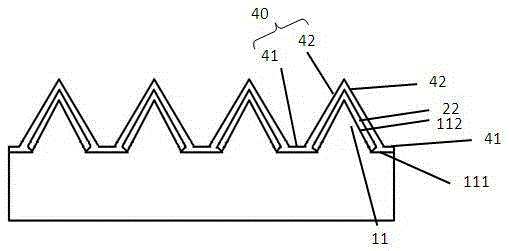
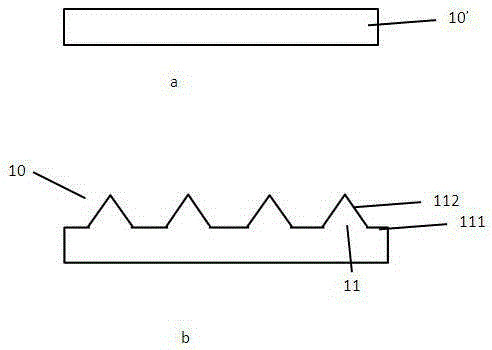
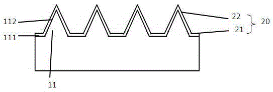
[0041] See attached figure 1, the patterned substrate 10 provided by the present invention, the patterned substrate 10 has an opposite first surface and a second surface, wherein the first surface is uniform and its surface is evenly distributed with a plurality of protrusions 11, and the adjacent protrusions The distance between the protrusions 11 is 50nm~5000nm, and there is no platform structure at the top of the protrusions 11, preferably a triangular pyramid structure. The side surface 112 of the protrusion 11 is deposited with a dielectric layer 22 with a thickness of 1 nm to 200 nm, while the gap surface 111 of the protrusion has no dielectric layer, and the dielectric layer 22 is any one of a silicon dioxide layer or a silicon nitride layer. The surface of the substrate with the dielectric layer 22 is deposited with an aluminum nitride layer 40 with a thickness of 1 nm to 200 nm. The aluminum nitride layer 40 covers the surface of the dielectric layer 22 of the protrus...

Embodiment 2

[0048] See attached Figure 8 and 9 , the difference between this embodiment and Embodiment 1 is that in this embodiment, the protrusion of the patterned substrate 10 also has a top platform 113 structure, and the protrusion 11 is a circular frustum structure, an elliptical frustum structure, and a prism structure. One: the dielectric layer 20 is not only deposited on the raised side surface 112, but also deposited on the raised top surface platform 113, and the aluminum nitride layer 40 in the subsequent process is also deposited on the raised gap surface 111 and the raised side surface 112 in sequence The surface of the dielectric layer 23 at the dielectric layer 22 and the raised platform 113; use the amorphous characteristics of the aluminum nitride layer 42 on the surface of the dielectric layer 22 and the aluminum nitride layer 43 on the surface of the top platform dielectric layer 23 and the raised gap surface 112 The crystalline properties of the aluminum nitride laye...


PUM

PropertyMeasurementUnit
Spacingaaaaaaaaaa
Thicknessaaaaaaaaaa

Abstract

The invention provides a patterned substrate, a preparation method and a light-emitting diode. A dielectric layer is deposited on the surface of the substrate with a plurality of bulges, and the amorphous body characteristic of the dielectric layer is utilized, so that aluminum nitride layers deposited on platforms on the side surfaces and top surfaces of the bulges through a PVD method are amorphous, and aluminum nitride arranged on the smooth surfaces of bulge gaps in a covering manner is polycrystal consisting of micro crystal particles. Then, when the substrate is applied to an MOCVD method to deposit gallium nitride-based epitaxial layers to form the light-emitting diode, by utilizing characteristics that the aluminum nitride polycrystal grows more easily on the smooth surfaces and the amorphous aluminum nitride is unlikely to deposit the gallium nitride-based epitaxial layers, the epitaxial layers selectively grow on the aluminum nitride layers on the smooth surfaces of the bulge gaps, and the platforms on the side surfaces and top surfaces of the bulges are unlikely to grow, so that the growth of the gallium nitride-based epitaxial layers on the side surfaces is reduced, the quantity of defects when the gallium nitride-based epitaxial layers in lateral growth and the gallium nitride-based epitaxial layers in positive growth on the smooth surfaces are merged is reduced, and the performance of the finally formed semiconductor element is promoted. Moreover, the growth of the lateral gallium nitride-based epitaxial layers is inhibited, and the gallium nitride-based epitaxial layers in positive growth are merged into a smooth surface more easily.

Description

technical field [0001] The invention belongs to the technical field of semiconductor manufacturing, and in particular relates to a patterned substrate for reducing crystal defects, a preparation method and a light-emitting diode. Background technique [0002] Now mainstream LEDs use patterned substrates for epitaxial growth. On the one hand, the pattern on the surface provides a variety of growth crystal phase options for the growth of the GaN epitaxial layer in the later stage, so that the GaN epitaxial layer is changed from the traditional two-dimensional The growth becomes three-dimensional growth, thereby effectively reducing the dislocation density in GaN-based LED materials, avoiding the generation of cracks, and improving the internal quantum luminous efficiency of LEDs; on the other hand, because the array pattern structure increases light scattering, The optical circuit of the LED is changed to form diffuse reflection, thereby improving the light extraction efficien...

Claims


Application Information

Patent Timeline
IPC IPC(8): H01L33/12H01L33/00
CPCH01L33/00H01L33/12H01L33/007
Inventor 徐志波李政鸿谢翔麟王肖
Owner ANHUI SANAN OPTOELECTRONICS CO LTD
Why Eureka
Try Eureka