Method for evaluating crystallinity of polycrystalline silicon

An evaluation method, polycrystalline silicon technology, applied in the direction of crystal growth, polycrystalline material growth, chemical instruments and methods, etc., can solve problems such as non-uniform melting, melting dependence on size, etc.

Inactive Publication Date: 2016-03-09
SHIN ETSU CHEM IND CO LTD
View PDF6 Cites 8 Cited by
  • Summary
  • Abstract
  • Description
  • Claims
  • Application Information

AI Technical Summary

Problems solved by technology

[0004] In addition, in Patent Document 2, in the process of manufacturing polycrystalline silicon rods (polycrystalline silicon rods, polycrystalline silicon rods) by the Siemens method, needle-like crystals may be precipitated in the rods, and single crystal silicon rods are produced by the FZ method using the polycrystalline silicon rods. During the cultivation, it was pointed out that there was a problem that the melting of each crystallite was dependent on its size, so that it could not be melted uniformly, and the unmelted crystallites passed through the melting region in the form of solid particles to the single crystal rod, so that the unmelted particles form is introduced into the solidification plane of the single crystal, thereby causing defect formation

Method used


Image

  • Method for evaluating crystallinity of polycrystalline silicon
  • Method for evaluating crystallinity of polycrystalline silicon
  • Method for evaluating crystallinity of polycrystalline silicon

Examples


Embodiment

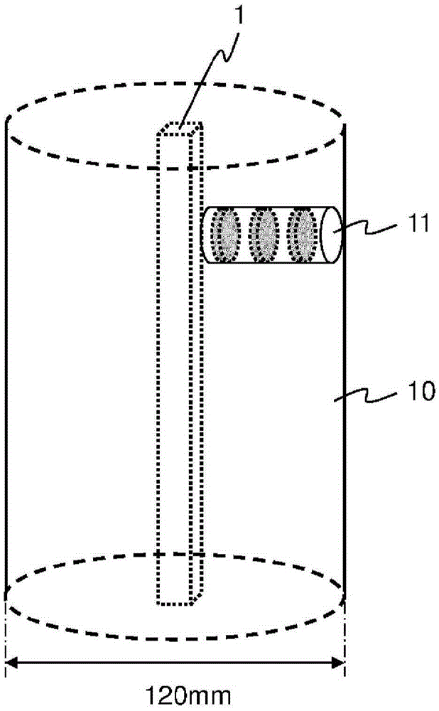
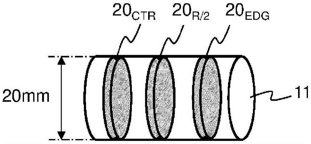
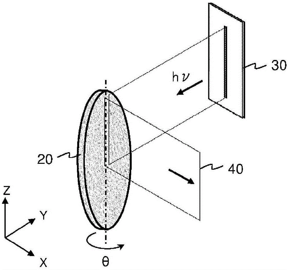
[0081] Prepare 13 polysilicon rods grown under different precipitation conditions. For these polysilicon rods (silicon rods 1 to 13), each from Figure 1A with 1B For the three positions shown, select disc-shaped samples (20 mm) with a thickness of about 2 mm. CTR 、20 EDG 、20 R / 2 ),pass Image 6 With the measurement system shown, the φ scanning diagrams of the Miller index surfaces and are obtained. In addition, the diameter of the disk-shaped sample 20 was about 20 mm.

[0082] It should be noted that the selection position of the plate sample is not limited to Figure 1A with 1B The three positions shown are, for example, positions within R / 3 from the center of the polysilicon rod of radius R, positions within 1R / 3 to 2R / 3, positions greater than 2R / 3 and within 3R / 3. three places.

[0083] Table 1 (Example) and Table 2 summarize the diffraction intensities of the baselines of each disk-shaped sample obtained from these polycrystalline silicon rods, an...


PUM

PropertyMeasurementUnit
diameteraaaaaaaaaa

Abstract

The present invention involves: positioning a collected plate-shaped specimen (20) in a position where a Bragg reflection from a first Miller index surface <h1k1l1> is detected; in-plane rotating the plate-shaped specimen (20) at a rotation angle (phi) with the center of the plate-shaped specimen (20) as the center of rotation in a manner such that the x-ray-irradiation region delimited by a slit phi-scans the principal surface of the plate-shaped specimen (20); obtaining a chart expressing the rotation-angle (phi) dependency of the plate-shaped specimen (20) of the Bragg reflection intensity from the Miller index surface <hkl>; obtaining a baseline diffraction intensity value (IB) from the chart; similarly obtaining a baseline diffraction intensity value (IB 2) from a phi-scan chart obtained from a second Miller index surface <h2k2l2>; and using the magnitude correlation between the IB 1 value and the IB 2 value as the evaluation indicator of the crystallinity of polycrystalline silicon.

Description

technical field [0001] The present invention relates to a method of evaluating the crystallinity of polycrystalline silicon by an X-ray diffraction method, and a method of selecting a polycrystalline silicon rod or a polycrystalline silicon block suitable as a raw material for stably producing single crystal silicon using the method. Background technique [0002] Monocrystalline silicon, which is indispensable in the manufacture of semiconductor devices, etc., is grown by the CZ method and the FZ method, and polycrystalline silicon rods and polycrystalline silicon blocks are used as raw materials at this time. Such polysilicon materials are often produced by the Siemens method (see Patent Document 1 and the like). The Siemens method refers to a method in which silane raw material gases such as trichlorosilane and monosilane are brought into contact with a heated silicon core wire, thereby depositing polysilicon on the surface of the silicon core wire by CVD (Chemical Vapor D...

Claims


Application Information

Patent Timeline
Patent Type & Authority Applications(China)
IPC IPC(8): G01N23/207C30B29/06C01B33/02
CPCC01B33/02C30B13/00C30B15/00C30B29/06C30B35/007C01P2002/70G01N23/207
Inventor 宫尾秀一祢津茂义
Owner SHIN ETSU CHEM IND CO LTD
Why Eureka
Try Eureka